Microfabrication by Light-Directed Electrokinetics on Semiconductor Electrodes at the Atomic and Molecular Scale: Principles, Materials, and Applications
IF 4.7 3区 材料科学Q1 ENGINEERING, ELECTRICAL & ELECTRONIC
Chenghan Zhao, Sen Li, Zibo Di, Xingbin Zhang, Xiaojie Tang and Wenzheng Wu*,
{"title":"Microfabrication by Light-Directed Electrokinetics on Semiconductor Electrodes at the Atomic and Molecular Scale: Principles, Materials, and Applications","authors":"Chenghan Zhao, Sen Li, Zibo Di, Xingbin Zhang, Xiaojie Tang and Wenzheng Wu*, ","doi":"10.1021/acsaelm.5c00386","DOIUrl":null,"url":null,"abstract":"<p >Light-directed electrokinetics-based technology, a fusion of optics, electrokinetics, and microfluidics, integrating the high-resolution dynamic directionality of light and precise and programmable layer-by-layer manufacturing of additive manufacturing, has been demonstrated to assemble and fabricate 3D structures rapidly without a mask at the microscale. In this paper, we present a comprehensive review of the precise fabrication of micro/nanoparticles by light-directed electrokinetics-based technology, including light-directed dielectrophoretic (LDD) and light-directed electrochemistry (LDE), which is capable of fabricating arbitrary custom shapes and microscale structures at precise locations onto a semiconductor surface by shaping the projected light pattern under ambient conditions with high efficiency. Besides, current challenges facing the light-directed electrokinetics technique and future possible innovations on it are also explained.</p>","PeriodicalId":3,"journal":{"name":"ACS Applied Electronic Materials","volume":"7 15","pages":"6733–6746"},"PeriodicalIF":4.7000,"publicationDate":"2025-07-01","publicationTypes":"Journal Article","fieldsOfStudy":null,"isOpenAccess":false,"openAccessPdf":"","citationCount":"0","resultStr":null,"platform":"Semanticscholar","paperid":null,"PeriodicalName":"ACS Applied Electronic Materials","FirstCategoryId":"88","ListUrlMain":"https://pubs.acs.org/doi/10.1021/acsaelm.5c00386","RegionNum":3,"RegionCategory":"材料科学","ArticlePicture":[],"TitleCN":null,"AbstractTextCN":null,"PMCID":null,"EPubDate":"","PubModel":"","JCR":"Q1","JCRName":"ENGINEERING, ELECTRICAL & ELECTRONIC","Score":null,"Total":0}
引用次数: 0
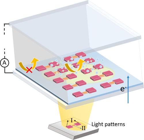
Abstract
Light-directed electrokinetics-based technology, a fusion of optics, electrokinetics, and microfluidics, integrating the high-resolution dynamic directionality of light and precise and programmable layer-by-layer manufacturing of additive manufacturing, has been demonstrated to assemble and fabricate 3D structures rapidly without a mask at the microscale. In this paper, we present a comprehensive review of the precise fabrication of micro/nanoparticles by light-directed electrokinetics-based technology, including light-directed dielectrophoretic (LDD) and light-directed electrochemistry (LDE), which is capable of fabricating arbitrary custom shapes and microscale structures at precise locations onto a semiconductor surface by shaping the projected light pattern under ambient conditions with high efficiency. Besides, current challenges facing the light-directed electrokinetics technique and future possible innovations on it are also explained.
期刊介绍:
ACS Applied Electronic Materials is an interdisciplinary journal publishing original research covering all aspects of electronic materials. The journal is devoted to reports of new and original experimental and theoretical research of an applied nature that integrate knowledge in the areas of materials science, engineering, optics, physics, and chemistry into important applications of electronic materials. Sample research topics that span the journal's scope are inorganic, organic, ionic and polymeric materials with properties that include conducting, semiconducting, superconducting, insulating, dielectric, magnetic, optoelectronic, piezoelectric, ferroelectric and thermoelectric.
Indexed/Abstracted:
Web of Science SCIE
Scopus
CAS
INSPEC
Portico

 求助内容:
求助内容: 应助结果提醒方式:


