Cheng Yi, Zejing Wang, Yangyang Shi, Shuai Wan, Jiao Tang, Wanlin Hu, Zile Li, Yongquan Zeng, Qinghua Song, Zhongyang Li
{"title":"Creating topological exceptional point by on-chip all-dielectric metasurface","authors":"Cheng Yi, Zejing Wang, Yangyang Shi, Shuai Wan, Jiao Tang, Wanlin Hu, Zile Li, Yongquan Zeng, Qinghua Song, Zhongyang Li","doi":"10.1038/s41377-025-01955-2","DOIUrl":null,"url":null,"abstract":"<p>Classified as a non-Hermitian system, topological metasurface is one of the ideal platforms for exploring a striking property, that is, the exceptional point (EP). Recently, creating and encircling EP in metasurfaces has triggered various progressive functionalities, including polarization control and optical holographic encoding. However, existing topological metasurfaces mostly rely on plasmonic materials, which introduce inevitable ohmic losses and limit their compatibility with mainstream all-dielectric meta-devices. Additionally, conventional free-space configurations also hinder the integration of multiple meta-devices in compact platforms. Here, an on-chip topological metasurface is experimentally demonstrated to create and engineer the topological phase encircling the EP in all-dielectric architecture. By massively screening the Si meta-atom geometry on the Si<sub>3</sub>N<sub>4</sub> waveguide, a 2π-topological phase shift is obtained by encircling the EP. Through combining with the Pancharatnam-Berry (PB) phase, we decouple the orthogonal circular polarization channels and unfold the independent encoding freedom for different holographic generations. As a proof of concept, the proposed on-chip topological metasurface enables floating holographic visualizations in real-world scenarios, functioning as practical augmented reality (AR) functionalities. Such the all-dielectric on-chip scheme eliminates ohmic losses and enables compatible integration with other on-chip meta-devices, thus suggesting promising applications in next-generation AR devices, multiplexing information storage, and advanced optical displays.</p>","PeriodicalId":18069,"journal":{"name":"Light-Science & Applications","volume":"29 1","pages":""},"PeriodicalIF":23.4000,"publicationDate":"2025-08-05","publicationTypes":"Journal Article","fieldsOfStudy":null,"isOpenAccess":false,"openAccessPdf":"","citationCount":"0","resultStr":null,"platform":"Semanticscholar","paperid":null,"PeriodicalName":"Light-Science & Applications","FirstCategoryId":"1089","ListUrlMain":"https://doi.org/10.1038/s41377-025-01955-2","RegionNum":0,"RegionCategory":null,"ArticlePicture":[],"TitleCN":null,"AbstractTextCN":null,"PMCID":null,"EPubDate":"","PubModel":"","JCR":"Q1","JCRName":"OPTICS","Score":null,"Total":0}
引用次数: 0
Abstract
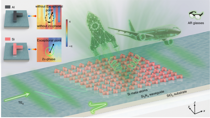
Classified as a non-Hermitian system, topological metasurface is one of the ideal platforms for exploring a striking property, that is, the exceptional point (EP). Recently, creating and encircling EP in metasurfaces has triggered various progressive functionalities, including polarization control and optical holographic encoding. However, existing topological metasurfaces mostly rely on plasmonic materials, which introduce inevitable ohmic losses and limit their compatibility with mainstream all-dielectric meta-devices. Additionally, conventional free-space configurations also hinder the integration of multiple meta-devices in compact platforms. Here, an on-chip topological metasurface is experimentally demonstrated to create and engineer the topological phase encircling the EP in all-dielectric architecture. By massively screening the Si meta-atom geometry on the Si3N4 waveguide, a 2π-topological phase shift is obtained by encircling the EP. Through combining with the Pancharatnam-Berry (PB) phase, we decouple the orthogonal circular polarization channels and unfold the independent encoding freedom for different holographic generations. As a proof of concept, the proposed on-chip topological metasurface enables floating holographic visualizations in real-world scenarios, functioning as practical augmented reality (AR) functionalities. Such the all-dielectric on-chip scheme eliminates ohmic losses and enables compatible integration with other on-chip meta-devices, thus suggesting promising applications in next-generation AR devices, multiplexing information storage, and advanced optical displays.
 求助内容:
求助内容: 应助结果提醒方式:


