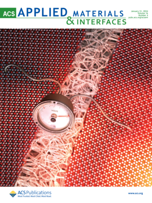
Correlating Carrier Localization to Optoelectronic Behavior of Monolayer MoS2.
IF 8.3
2区 材料科学
Q1 MATERIALS SCIENCE, MULTIDISCIPLINARY
引用次数: 0
Abstract
In nanoscale semiconductor devices, electrical conductivity is significantly influenced by inherent disorder. This study examines the electrical transport properties of a single-layer MoS2 field-effect transistor on a few-layered hBN substrate. Temperature-dependent transport measurements reveal that electrical conductivity is predominantly governed by a combination of simple activated and variable-range hopping mechanisms. The calculations on the experimental data yield a localization length around 5 nm for a typical defect density near the Fermi energy as 1014 eVcm-2. Additionally, optoelectronic transport measurements exhibit temperature-dependent persistent photoconductivity, attributed to electron localization within defect states. Calculations based on the temperature-dependent photoconductivity relaxation indicate a localization length of 7 nm, suggesting a direct correlation between the two phenomena.载流子定位与单层二硫化钼光电性能的关系。
在纳米级半导体器件中,导电性受到固有无序的显著影响。本研究考察了单层MoS2场效应晶体管在多层hBN衬底上的电输运特性。温度相关输运测量表明,电导率主要由简单激活和可变范围跳变机制的组合控制。对实验数据的计算得出在费米能量附近典型缺陷密度为1014 eVcm-2的局域化长度约为5 nm。此外,光电输运测量显示出温度依赖的持久光电导率,归因于缺陷状态内的电子局部化。基于温度相关光电导弛豫的计算表明,局域化长度为7 nm,表明这两种现象之间存在直接关联。
本文章由计算机程序翻译,如有差异,请以英文原文为准。
求助全文
约1分钟内获得全文
求助全文
来源期刊

ACS Applied Materials & Interfaces
工程技术-材料科学:综合
CiteScore
16.00
自引率
6.30%
发文量
4978
审稿时长
1.8 months
期刊介绍:
ACS Applied Materials & Interfaces is a leading interdisciplinary journal that brings together chemists, engineers, physicists, and biologists to explore the development and utilization of newly-discovered materials and interfacial processes for specific applications. Our journal has experienced remarkable growth since its establishment in 2009, both in terms of the number of articles published and the impact of the research showcased. We are proud to foster a truly global community, with the majority of published articles originating from outside the United States, reflecting the rapid growth of applied research worldwide.
 求助内容:
求助内容: 应助结果提醒方式:


