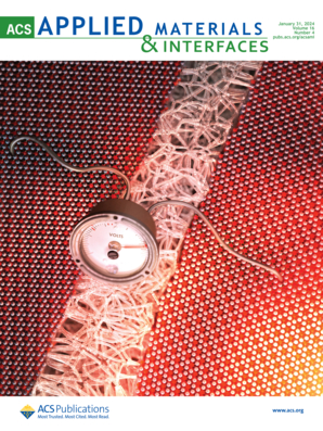
Recyclable Ctenophore-Inspired Field-Coupling Microspheres for Precise Detection of Microscopic Defects and Electric Field Distortions in Dielectric Materials.
IF 8.3
2区 材料科学
Q1 MATERIALS SCIENCE, MULTIDISCIPLINARY
引用次数: 0
Abstract
Microscopic defects within dielectrics can distort the local electric field at the operating voltage, inducing electrical aging or even insulation failure. These defects are only a few hundred micrometers, and the corresponding distorted electric fields are extremely weak. Consequently, it is challengeable for existing sensing methods to detect these defects and distorted electric fields accurately, in situ, and nondestructively under electrically charged conditions. Inspired by the warning bioluminescence of ctenophores, we designed a field-coupling microsphere (FCM) with high sensitivity of microscopic defects and distorted electric fields. When the FCM is located in a distorted electric field, the micron-scale luminescent units on its surface precisely sense this distorted electric field and emit in situ electroluminescence, thus exposing defects and distorted electric fields. Furthermore, we prepared a recyclable electrosensitive coating (REC) by compounding FCMs into phase-change matrix materials that are applicable to the surfaces of electrical and electronic equipment to accurately sense microscopic defects and distorted electric fields. To the best of our knowledge, this is the first smart coating material to visualize invisible distorted electric fields using field-coupled electroluminescence, which provides a novel method to study electric field evolution inside dielectrics and to detect microscopic defects in electrical and electronic equipment.用于精确检测介电材料微观缺陷和电场畸变的可回收栉水母激发场耦合微球。
电介质内部的微小缺陷会在工作电压下扭曲局部电场,导致电老化甚至绝缘失效。这些缺陷只有几百微米,相应的畸变电场非常微弱。因此,现有的传感方法很难在带电条件下准确、原位、无损地检测这些缺陷和扭曲的电场。受栉水母警告性生物发光的启发,我们设计了一种对微观缺陷和畸变电场具有高灵敏度的场耦合微球(FCM)。当FCM处于扭曲的电场中时,其表面的微米级发光单元精确地感知扭曲的电场并发出原位电致发光,从而暴露缺陷和扭曲的电场。此外,我们将fcm复合到相变基质材料中,制备了一种可回收的电敏感涂层(REC),该涂层适用于电气和电子设备表面,可以准确地感知微观缺陷和畸变电场。据我们所知,这是第一种使用场耦合电致发光来可视化不可见扭曲电场的智能涂层材料,它为研究电介质内部的电场演变以及检测电气和电子设备的微观缺陷提供了一种新方法。
本文章由计算机程序翻译,如有差异,请以英文原文为准。
求助全文
约1分钟内获得全文
求助全文
来源期刊

ACS Applied Materials & Interfaces
工程技术-材料科学:综合
CiteScore
16.00
自引率
6.30%
发文量
4978
审稿时长
1.8 months
期刊介绍:
ACS Applied Materials & Interfaces is a leading interdisciplinary journal that brings together chemists, engineers, physicists, and biologists to explore the development and utilization of newly-discovered materials and interfacial processes for specific applications. Our journal has experienced remarkable growth since its establishment in 2009, both in terms of the number of articles published and the impact of the research showcased. We are proud to foster a truly global community, with the majority of published articles originating from outside the United States, reflecting the rapid growth of applied research worldwide.
 求助内容:
求助内容: 应助结果提醒方式:


