Junaid Khan, Júlia Marí-Guaita, Kenneth Lobo, Giovanni Vescio, Carina Pareja-Rivera, Iván Mora-Seró, Sergi Hernández, Albert Cirera and Blas Garrido
{"title":"Effect of annealing temperature on the properties of CsPbBr3 nanocrystal films via inkjet printing and its application in colour conversion layers†","authors":"Junaid Khan, Júlia Marí-Guaita, Kenneth Lobo, Giovanni Vescio, Carina Pareja-Rivera, Iván Mora-Seró, Sergi Hernández, Albert Cirera and Blas Garrido","doi":"10.1039/D5NR01385B","DOIUrl":null,"url":null,"abstract":"<p >Inkjet printing has emerged as a sustainable and scalable approach for fabricating electronic and optoelectronic devices, offering precise material deposition with minimal waste. Among solution-processable materials, metal halide perovskites, particularly CsPbBr<small><sub>3</sub></small>, have gained significant attention due to their exceptional optoelectronic properties, including high photoluminescence quantum yield, tuneable bandgap, and efficient charge transport. However, optimizing the inkjet-printing process remains a challenge, particularly post printing annealing since CsPbBr<small><sub>3</sub></small> nanocrystals are sensitive to environmental conditions. In this study, we systematically investigate the effect of annealing temperature on the structural, morphological, and photoluminescence properties of inkjet-printed CsPbBr<small><sub>3</sub></small> films. Our results reveal that thermal treatment plays a pivotal role in controlling grain size, crystallinity, defect density, and overall optoelectronic behaviour. Notably, a remarkable 70-fold enhancement in photoluminescence emission was observed, alongside a crystal structure morphology evolution from 3D to 0D and 2D structures through simple annealing offering transformative potential for optoelectronic applications. By elucidating the interplay between annealing conditions and film characteristics, this work provides key insights for optimizing inkjet-printed perovskite films, driving advancements in next-generation, sustainable, and high-performance printed electronics. The application of the printed films was successfully demonstrated as efficient colour conversion layers for optoelectronic devices.</p>","PeriodicalId":92,"journal":{"name":"Nanoscale","volume":" 30","pages":" 17803-17815"},"PeriodicalIF":5.1000,"publicationDate":"2025-07-21","publicationTypes":"Journal Article","fieldsOfStudy":null,"isOpenAccess":false,"openAccessPdf":"https://pubs.rsc.org/en/content/articlepdf/2025/nr/d5nr01385b?page=search","citationCount":"0","resultStr":null,"platform":"Semanticscholar","paperid":null,"PeriodicalName":"Nanoscale","FirstCategoryId":"88","ListUrlMain":"https://pubs.rsc.org/en/content/articlelanding/2025/nr/d5nr01385b","RegionNum":3,"RegionCategory":"材料科学","ArticlePicture":[],"TitleCN":null,"AbstractTextCN":null,"PMCID":null,"EPubDate":"","PubModel":"","JCR":"Q1","JCRName":"CHEMISTRY, MULTIDISCIPLINARY","Score":null,"Total":0}
引用次数: 0
Abstract
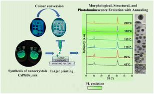
Inkjet printing has emerged as a sustainable and scalable approach for fabricating electronic and optoelectronic devices, offering precise material deposition with minimal waste. Among solution-processable materials, metal halide perovskites, particularly CsPbBr3, have gained significant attention due to their exceptional optoelectronic properties, including high photoluminescence quantum yield, tuneable bandgap, and efficient charge transport. However, optimizing the inkjet-printing process remains a challenge, particularly post printing annealing since CsPbBr3 nanocrystals are sensitive to environmental conditions. In this study, we systematically investigate the effect of annealing temperature on the structural, morphological, and photoluminescence properties of inkjet-printed CsPbBr3 films. Our results reveal that thermal treatment plays a pivotal role in controlling grain size, crystallinity, defect density, and overall optoelectronic behaviour. Notably, a remarkable 70-fold enhancement in photoluminescence emission was observed, alongside a crystal structure morphology evolution from 3D to 0D and 2D structures through simple annealing offering transformative potential for optoelectronic applications. By elucidating the interplay between annealing conditions and film characteristics, this work provides key insights for optimizing inkjet-printed perovskite films, driving advancements in next-generation, sustainable, and high-performance printed electronics. The application of the printed films was successfully demonstrated as efficient colour conversion layers for optoelectronic devices.
期刊介绍:
Nanoscale is a high-impact international journal, publishing high-quality research across nanoscience and nanotechnology. Nanoscale publishes a full mix of research articles on experimental and theoretical work, including reviews, communications, and full papers.Highly interdisciplinary, this journal appeals to scientists, researchers and professionals interested in nanoscience and nanotechnology, quantum materials and quantum technology, including the areas of physics, chemistry, biology, medicine, materials, energy/environment, information technology, detection science, healthcare and drug discovery, and electronics.

 求助内容:
求助内容: 应助结果提醒方式:


