Potential of ultrahigh-vacuum based surface treatments in silicon technology
IF 3.1
4区 工程技术
Q2 ENGINEERING, ELECTRICAL & ELECTRONIC
引用次数: 0
Abstract
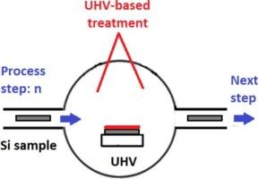
Ultrahigh vacuum (UHV) environment with the background pressure in the range of 1‧10−15–1‧10−11 bar is common in surface-science experiments, but UHV-based material treatments are rarely used in the current silicon technology. UHV methods might however provide a clear benefit to the technology when atomic-level cleanliness and crystalline order of Si surfaces (interfaces) as well as dry-cleaning methods for the surfaces become relevant to the development of Si devices. We have studied effects of some UHV-based treatments on the properties of Si surfaces and of thin oxide films on Si. Exposing Si, pre-cleaned by the RCA recipe with the final HF dip, to mere hydrogen (H2) gas in UHV chamber at the Si temperature of 200 °C increases a crystalline degree of the Si surface according to low-energy electron diffraction. Effects of postheating in UHV are also studied for different oxidized Si surfaces. Wet chemically oxidized (RCA without HF dip) Si was heated step-by-step up to 800 °C in UHV until the oxide removal is strongly enhanced. Both crystalline degree of the RCA chemical oxide and surface roughness increase with the UHV post-heating at 500–800 °C. Exposing native-oxide covered sidewalls of Si diodes to mere oxygen (O2) gas in UHV chamber at Si temperature of 350 °C (i) increases amount of SiO2 at the sidewalls according to x-ray photoelectron spectroscopy, (ii) decreases amount of the band-gap electron levels at the sidewalls according to scanning tunneling spectroscopy, and (iii) provides a durable decrease in the diode leakage current.
超高真空基表面处理在硅技术中的潜力
背景压力在1·10−15-1·10−11 bar范围内的超高真空(UHV)环境在表面科学实验中很常见,但在当前的硅技术中很少使用基于UHV的材料处理。然而,当硅表面(界面)的原子级清洁度和晶体顺序以及表面的干洗方法与硅器件的发展相关时,特高压方法可能会为该技术提供明显的好处。我们研究了几种超高压处理对硅表面和硅表面氧化薄膜性能的影响。根据低能电子衍射结果,用RCA配方预清洗后的Si在200°C的超高压室中暴露于纯氢(H2)气体中,增加了Si表面的结晶度。此外,还研究了不同氧化硅表面在特高压条件下的置热效应。湿化学氧化(RCA无HF浸)Si在特高压下逐步加热至800°C,直到氧化物的去除得到强烈增强。RCA化学氧化物的结晶度和表面粗糙度随着500 ~ 800℃特高压后加热的增加而增加。将天然氧化物覆盖的硅二极管侧壁在350℃的特高压室中暴露于纯氧(O2)气体中(i)根据x射线光电子能谱增加了侧壁SiO2的含量,(ii)根据扫描隧道能谱降低了侧壁带隙电子能级的数量,(iii)提供了二极管泄漏电流的持久降低。
本文章由计算机程序翻译,如有差异,请以英文原文为准。
求助全文
约1分钟内获得全文
求助全文
来源期刊

Microelectronic Engineering
工程技术-工程:电子与电气
CiteScore
5.30
自引率
4.30%
发文量
131
审稿时长
29 days
期刊介绍:
Microelectronic Engineering is the premier nanoprocessing, and nanotechnology journal focusing on fabrication of electronic, photonic, bioelectronic, electromechanic and fluidic devices and systems, and their applications in the broad areas of electronics, photonics, energy, life sciences, and environment. It covers also the expanding interdisciplinary field of "more than Moore" and "beyond Moore" integrated nanoelectronics / photonics and micro-/nano-/bio-systems. Through its unique mixture of peer-reviewed articles, reviews, accelerated publications, short and Technical notes, and the latest research news on key developments, Microelectronic Engineering provides comprehensive coverage of this exciting, interdisciplinary and dynamic new field for researchers in academia and professionals in industry.
 求助内容:
求助内容: 应助结果提醒方式:


