{"title":"0.26-inch LED microdisplay using pixel level Cu–Cu connections of transferred GaN/Si and CMOS backplane wafer","authors":"Haruki Tsuchiya, Toshihiro Miura, Ryosuke Matsumoto, Mikio Takiguchi, Toru Sasaki, Michihiro Kanno, Koichi Nagasawa, Hayato Iwamoto","doi":"10.1002/jsid.2071","DOIUrl":null,"url":null,"abstract":"<p>We have developed an integration process for LED microdisplays toward augmented reality (AR) applications and present the first demonstration of a blue mono-color active-matrix LED microdisplay fabricated with this process methodology. One of the primary manufacturing challenges in realizing LED microdisplays is to develop a process that provides pixel-level heterogeneous connections between III-V compound LEDs and Si CMOS circuits at a fine pixel pitch. In this work, a die-to-silicon process is employed, in which GaN on Si chips are reconstituted on a larger-diameter support Si wafer (referred to as GaN/Si wafer), allowing the use of Si CMOS wafer processes, including novel Cu-Cu hybridization. After the Cu-Cu hybridization process to bond a die-to-silicon transferred GaN/Si wafer and a Si CMOS backplane wafer, LED mesas and on-chip lenses (OCLs) are fabricated. We achieved high yields of pixel-level connections at 3.8-μm and 4.5-μm pitches through the Cu-Cu hybridization. Finely tapered 1.2-μm LED mesas with OCLs exhibited a 4.2-fold enhancement in light extraction efficiency (LEE) compared with a Lambertian emitter within the emission angle of ±20°. Also, we introduce the key features and results of the prototyped 0.26-in., 5,644-ppi LED microdisplay.</p>","PeriodicalId":49979,"journal":{"name":"Journal of the Society for Information Display","volume":"33 5","pages":"425-432"},"PeriodicalIF":2.2000,"publicationDate":"2025-04-03","publicationTypes":"Journal Article","fieldsOfStudy":null,"isOpenAccess":false,"openAccessPdf":"","citationCount":"0","resultStr":null,"platform":"Semanticscholar","paperid":null,"PeriodicalName":"Journal of the Society for Information Display","FirstCategoryId":"5","ListUrlMain":"https://sid.onlinelibrary.wiley.com/doi/10.1002/jsid.2071","RegionNum":4,"RegionCategory":"工程技术","ArticlePicture":[],"TitleCN":null,"AbstractTextCN":null,"PMCID":null,"EPubDate":"","PubModel":"","JCR":"Q3","JCRName":"ENGINEERING, ELECTRICAL & ELECTRONIC","Score":null,"Total":0}
引用次数: 0
Abstract
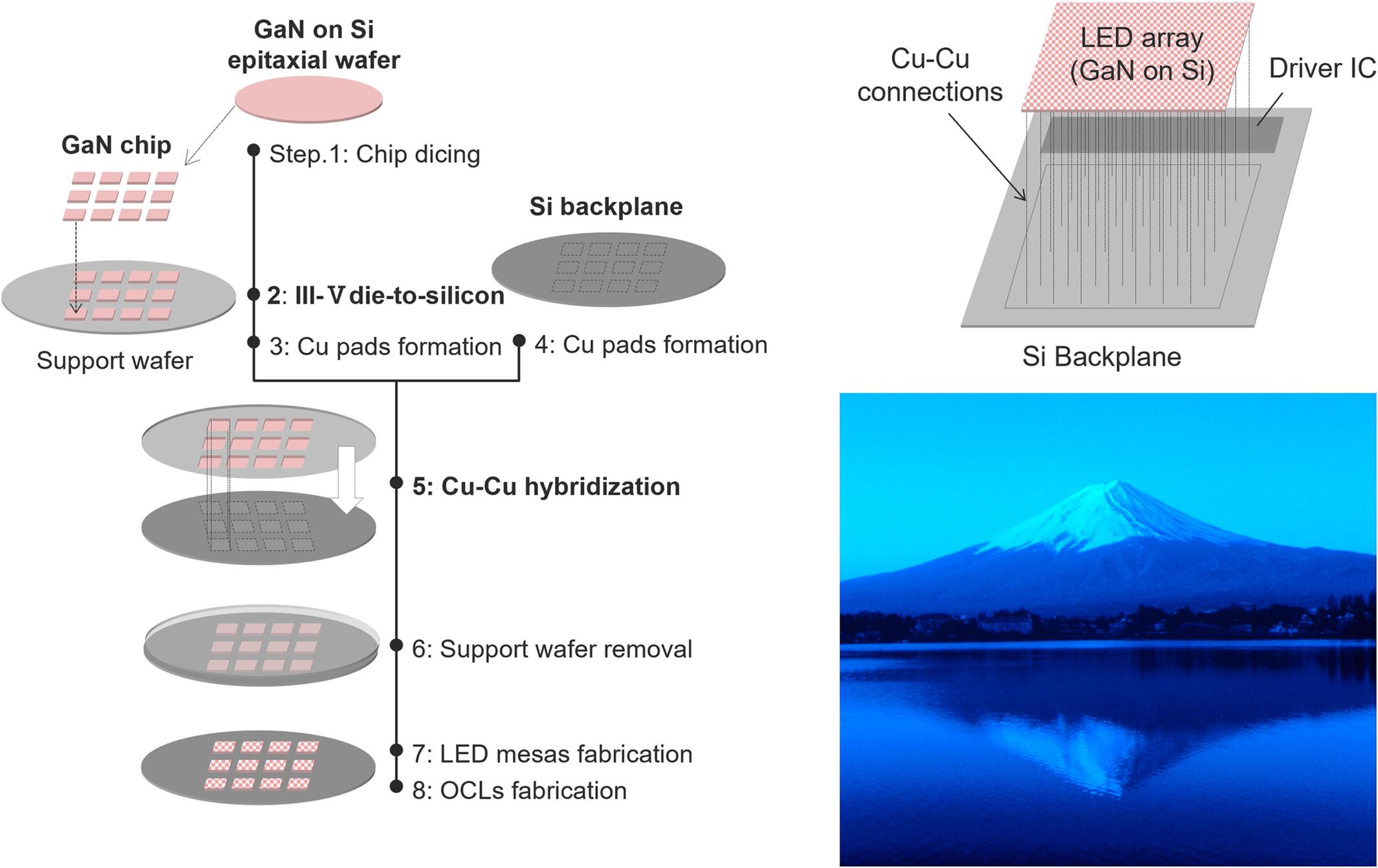
We have developed an integration process for LED microdisplays toward augmented reality (AR) applications and present the first demonstration of a blue mono-color active-matrix LED microdisplay fabricated with this process methodology. One of the primary manufacturing challenges in realizing LED microdisplays is to develop a process that provides pixel-level heterogeneous connections between III-V compound LEDs and Si CMOS circuits at a fine pixel pitch. In this work, a die-to-silicon process is employed, in which GaN on Si chips are reconstituted on a larger-diameter support Si wafer (referred to as GaN/Si wafer), allowing the use of Si CMOS wafer processes, including novel Cu-Cu hybridization. After the Cu-Cu hybridization process to bond a die-to-silicon transferred GaN/Si wafer and a Si CMOS backplane wafer, LED mesas and on-chip lenses (OCLs) are fabricated. We achieved high yields of pixel-level connections at 3.8-μm and 4.5-μm pitches through the Cu-Cu hybridization. Finely tapered 1.2-μm LED mesas with OCLs exhibited a 4.2-fold enhancement in light extraction efficiency (LEE) compared with a Lambertian emitter within the emission angle of ±20°. Also, we introduce the key features and results of the prototyped 0.26-in., 5,644-ppi LED microdisplay.
期刊介绍:
The Journal of the Society for Information Display publishes original works dealing with the theory and practice of information display. Coverage includes materials, devices and systems; the underlying chemistry, physics, physiology and psychology; measurement techniques, manufacturing technologies; and all aspects of the interaction between equipment and its users. Review articles are also published in all of these areas. Occasional special issues or sections consist of collections of papers on specific topical areas or collections of full length papers based in part on oral or poster presentations given at SID sponsored conferences.


 求助内容:
求助内容: 应助结果提醒方式:


