Actinic defect inspection and characterization for extreme ultraviolet mask blanks
IF 3.1
4区 工程技术
Q2 ENGINEERING, ELECTRICAL & ELECTRONIC
引用次数: 0
Abstract
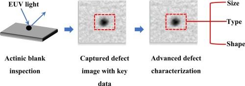
Extreme ultraviolet (EUV) lithography is crucial for advanced semiconductor manufacturing, relying on sophisticated mask technology to transfer intricate patterns onto silicon wafers. The integrity of the EUV mask blanks is essential for producing high-quality masks and semiconductor devices. However, defects in mask blanks, particularly multilayer phase defects, can significantly degrade lithographic quality, affecting device yield and performance. Actinic blank inspection (ABI) has emerged as the most effective strategy for evaluating the initial quality of EUV mask blanks and identifying defects that may compromise the wafer integrity. Additionally, defect characterization helps determine the nature of the defect, its printability, and its potential for repair. This review surveys recent advancements in ABI and defect characterization, covering a range of methodologies, commercial inspection tools and related research efforts that aimed at improving the detection and characterization of multilayer defects.
极紫外掩模毛坯的光化缺陷检测与表征
极紫外(EUV)光刻技术对于先进的半导体制造至关重要,它依靠复杂的掩模技术将复杂的图案转移到硅片上。EUV掩模毛坯的完整性对于生产高质量的掩模和半导体器件至关重要。然而,掩模毛坯中的缺陷,特别是多层相缺陷,会显著降低光刻质量,影响器件的良率和性能。光化毛坯检测(ABI)已成为评估EUV掩模毛坯初始质量和识别可能影响晶圆完整性的缺陷的最有效策略。此外,缺陷特征有助于确定缺陷的性质、可印刷性和修复潜力。本文综述了ABI和缺陷表征的最新进展,涵盖了一系列的方法、商业检测工具和相关的研究工作,旨在提高多层缺陷的检测和表征。
本文章由计算机程序翻译,如有差异,请以英文原文为准。
求助全文
约1分钟内获得全文
求助全文
来源期刊

Microelectronic Engineering
工程技术-工程:电子与电气
CiteScore
5.30
自引率
4.30%
发文量
131
审稿时长
29 days
期刊介绍:
Microelectronic Engineering is the premier nanoprocessing, and nanotechnology journal focusing on fabrication of electronic, photonic, bioelectronic, electromechanic and fluidic devices and systems, and their applications in the broad areas of electronics, photonics, energy, life sciences, and environment. It covers also the expanding interdisciplinary field of "more than Moore" and "beyond Moore" integrated nanoelectronics / photonics and micro-/nano-/bio-systems. Through its unique mixture of peer-reviewed articles, reviews, accelerated publications, short and Technical notes, and the latest research news on key developments, Microelectronic Engineering provides comprehensive coverage of this exciting, interdisciplinary and dynamic new field for researchers in academia and professionals in industry.
 求助内容:
求助内容: 应助结果提醒方式:


