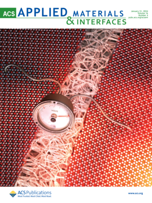
Making Use of Si Contaminants during Chemical Vapor Deposition of Graphene on Cu: Synthesis of a Stable Material with the Textbook-like Band Structure of Free-Standing Graphene.
IF 8.2
2区 材料科学
Q1 MATERIALS SCIENCE, MULTIDISCIPLINARY
引用次数: 0
Abstract
We report on a gentle procedure for the complete electronic decoupling of graphene from Cu. The procedure can be added to the growth protocol of graphene synthesis by chemical vapor deposition making use of the widely unnoticed silicon release from hot wall quartz tube reactors. So far, Si release was observed if the effect was large, so that it deteriorates the grown graphene. However, the effect can also be used to turn the electronic band structure of CVD-grown graphene on Cu into that of free-standing graphene as shown in a combined spectroscopic photoelectron and low energy electron microscopy study. Adding a foil pretreatment to the synthesis protocol in the reactor turns the polycrystalline foil into (111)-textured Cu, and the electronic band structure of CVD-grown graphene on Cu(111) is achieved with n-doping by -0.4 eV and band gap formation of 0.3 eV. If, however, graphene is synthesized on a Si-loaded Cu foil, subsequent oxygen exposure in the reactor segregates the dissolved Si to the surface and converts it to intercalated silica without destroying the covering graphene. The graphene decouples electronically, and the textbook-like electronic band structure of free-standing graphene emerges. The alternating stacking of 30°-rotated layers in thicker graphene leads to electronically noninteracting layers. Moreover, in angle-resolved photoemission, replica bands due to Umklapp processes emerge without the opening of an energy gap.石墨烯在Cu上化学气相沉积过程中硅污染物的利用:一种具有教科书式独立石墨烯带结构的稳定材料的合成。
我们报告了石墨烯与铜完全电子解耦的一种温和程序。该过程可以添加到化学气相沉积法合成石墨烯的生长方案中,利用热壁石英管反应器中广泛未被注意的硅释放。到目前为止,如果影响较大,则观察到Si释放,从而使生长的石墨烯变质。然而,该效应也可以用来将cvd生长的石墨烯在Cu上的电子带结构转变为独立石墨烯的电子带结构,如光电子和低能电子显微镜联合研究所示。在反应器中加入箔预处理,将多晶箔转化为(111)织体Cu,在-0.4 eV n掺杂和0.3 eV带隙形成的条件下,cvd生长的石墨烯在Cu(111)上获得了电子能带结构。然而,如果石墨烯是在硅负载的铜箔上合成的,随后在反应器中的氧气暴露将溶解的硅分离到表面,并将其转化为插层二氧化硅,而不会破坏覆盖的石墨烯。石墨烯在电子上解耦,出现了类似教科书的独立石墨烯电子带结构。在较厚的石墨烯中交替堆叠30°旋转层导致电子非相互作用层。此外,在角度分辨光发射中,由于Umklapp过程而产生的复制带没有打开能量间隙。
本文章由计算机程序翻译,如有差异,请以英文原文为准。
求助全文
约1分钟内获得全文
求助全文
来源期刊

ACS Applied Materials & Interfaces
工程技术-材料科学:综合
CiteScore
16.00
自引率
6.30%
发文量
4978
审稿时长
1.8 months
期刊介绍:
ACS Applied Materials & Interfaces is a leading interdisciplinary journal that brings together chemists, engineers, physicists, and biologists to explore the development and utilization of newly-discovered materials and interfacial processes for specific applications. Our journal has experienced remarkable growth since its establishment in 2009, both in terms of the number of articles published and the impact of the research showcased. We are proud to foster a truly global community, with the majority of published articles originating from outside the United States, reflecting the rapid growth of applied research worldwide.
 求助内容:
求助内容: 应助结果提醒方式:


