{"title":"Laser-Directed Bubble Printing of MXene-Based Composites: A Simple Route to Micropatterned Photodetectors","authors":"Marcel Herber, Bianca M. Hanly and Eric H. Hill*, ","doi":"10.1021/acsami.5c08769","DOIUrl":null,"url":null,"abstract":"<p >MXenes are a family of robust two-dimensional materials with tunable optical properties and high electrical conductivity ideal for optoelectronics. Herein, the direct, free-form micropatterning of MXene/semiconductor composites on glass substrates using a laser-driven microbubble is reported. As a proof-of-concept for the fabrication of photodetectors, this approach was used to print 0.09 mm<sup>2</sup> square patches of Ti<sub>3</sub>C<sub>2</sub>T<sub>X</sub> MXene combined with a number of different semiconductors. MXene composites printed with In<sub>2</sub>S<sub>3</sub> at different ratios revealed that a 9:1 MXene:In<sub>2</sub>S<sub>3</sub> ratio had increased responsivity compared to lower ratios or MXene alone. Out of the semiconductors studied, CsPbBr<sub>3</sub> halide perovskite nanocrystals gave the highest responsivity value of 21.3 mA/cm<sup>2</sup> under 369 nm illumination. Bubble printing of mixed colloids into micropatterned composite materials for photodetectors has great potential to advance sensing technologies across the electromagnetic spectrum while also requiring further optimization to enhance device performance. Overall, this further advances the application of MXenes in electronic and sensing devices, laying the foundation for future developments in patterning of miniaturized photodetectors.</p>","PeriodicalId":5,"journal":{"name":"ACS Applied Materials & Interfaces","volume":"17 26","pages":"38269–38279"},"PeriodicalIF":8.2000,"publicationDate":"2025-06-23","publicationTypes":"Journal Article","fieldsOfStudy":null,"isOpenAccess":false,"openAccessPdf":"https://pubs.acs.org/doi/pdf/10.1021/acsami.5c08769","citationCount":"0","resultStr":null,"platform":"Semanticscholar","paperid":null,"PeriodicalName":"ACS Applied Materials & Interfaces","FirstCategoryId":"88","ListUrlMain":"https://pubs.acs.org/doi/10.1021/acsami.5c08769","RegionNum":2,"RegionCategory":"材料科学","ArticlePicture":[],"TitleCN":null,"AbstractTextCN":null,"PMCID":null,"EPubDate":"","PubModel":"","JCR":"Q1","JCRName":"MATERIALS SCIENCE, MULTIDISCIPLINARY","Score":null,"Total":0}
引用次数: 0
Abstract
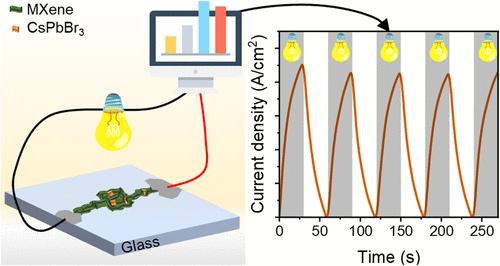
MXenes are a family of robust two-dimensional materials with tunable optical properties and high electrical conductivity ideal for optoelectronics. Herein, the direct, free-form micropatterning of MXene/semiconductor composites on glass substrates using a laser-driven microbubble is reported. As a proof-of-concept for the fabrication of photodetectors, this approach was used to print 0.09 mm2 square patches of Ti3C2TX MXene combined with a number of different semiconductors. MXene composites printed with In2S3 at different ratios revealed that a 9:1 MXene:In2S3 ratio had increased responsivity compared to lower ratios or MXene alone. Out of the semiconductors studied, CsPbBr3 halide perovskite nanocrystals gave the highest responsivity value of 21.3 mA/cm2 under 369 nm illumination. Bubble printing of mixed colloids into micropatterned composite materials for photodetectors has great potential to advance sensing technologies across the electromagnetic spectrum while also requiring further optimization to enhance device performance. Overall, this further advances the application of MXenes in electronic and sensing devices, laying the foundation for future developments in patterning of miniaturized photodetectors.
期刊介绍:
ACS Applied Materials & Interfaces is a leading interdisciplinary journal that brings together chemists, engineers, physicists, and biologists to explore the development and utilization of newly-discovered materials and interfacial processes for specific applications. Our journal has experienced remarkable growth since its establishment in 2009, both in terms of the number of articles published and the impact of the research showcased. We are proud to foster a truly global community, with the majority of published articles originating from outside the United States, reflecting the rapid growth of applied research worldwide.

 求助内容:
求助内容: 应助结果提醒方式:


