Bhishma Pandit, Jungwoo Bong, Seongwon Lee, Jungwoo Lee, Sameer Pokhrel, Hagyoul Bae, Ji-Wan Kim, Yunjo Jeong, Sangmin An, Jaehee Cho, Chel-Jong Choi, Krishna Moorthy Ponnusamy, S. Chandramohan, Hyeon-Sik Jang* and Keun Heo*,
{"title":"Photodetection Mechanisms and Ultraviolet–Visible Imaging Characteristics of High-Detectivity Broadband Metal–Semiconductor–Metal Photodetector Arrays on Wafer-Scale Monolayer MoS2","authors":"Bhishma Pandit, Jungwoo Bong, Seongwon Lee, Jungwoo Lee, Sameer Pokhrel, Hagyoul Bae, Ji-Wan Kim, Yunjo Jeong, Sangmin An, Jaehee Cho, Chel-Jong Choi, Krishna Moorthy Ponnusamy, S. Chandramohan, Hyeon-Sik Jang* and Keun Heo*, ","doi":"10.1021/acsami.5c0460210.1021/acsami.5c04602","DOIUrl":null,"url":null,"abstract":"<p >The discovery of an intrinsic direct bandgap in single-layer MoS<sub>2</sub> has revealed significant potential for advancements in optoelectronic and photonic applications. This study aims to explore this potential by developing a high-performance Ni/Au metal–semiconductor–metal photodetector on wafer-scale epitaxially grown MoS<sub>2</sub>. The quality of the monolayer MoS<sub>2</sub> film was verified using various techniques, including Raman, photoluminescence (PL), atomic force microscopy (AFM), X-ray photoelectron spectroscopy (XPS), and transmission electron microscopy (TEM). Results showed a high photoresponse of 2.06 and 0.68 A/W under 350 and 650 nm light illumination, respectively, at a 10 V reverse bias, along with an ultralow dark current measured in picoamps. These results indicate a low noise level and high photo-to-dark current rejection ratios of 5.45 × 10<sup>4</sup> and 3.41 × 10<sup>4</sup> under 350 and 650 nm illumination, respectively. The photodetector exhibited a maximum detectivity of 5.1 × 10<sup>16</sup> cm Hz<sup>1/2</sup> W<sup>–1</sup> at 5 V under 350 nm of UV illumination, and the quantum efficiency surpassed 100% when the reverse bias voltage exceeded 3 V, demonstrating gain manifestation within the device. The dominance of a trap-assisted photoconductive gain mechanism was suggested by the power law exponent and the temporal characteristics observed. UV and visible imaging capabilities were also demonstrated using a “MoS2”-printed shadow mask and a single metal–semiconductor–metal (MSM) photodetector. This study highlights the superior photoimaging capabilities of the MoS<sub>2</sub> MSM photodetector, offering substantial contributions to the field of optoelectronics and suggesting practical applications in photonic devices.</p>","PeriodicalId":5,"journal":{"name":"ACS Applied Materials & Interfaces","volume":"17 24","pages":"35732–35742 35732–35742"},"PeriodicalIF":8.2000,"publicationDate":"2025-06-06","publicationTypes":"Journal Article","fieldsOfStudy":null,"isOpenAccess":false,"openAccessPdf":"","citationCount":"0","resultStr":null,"platform":"Semanticscholar","paperid":null,"PeriodicalName":"ACS Applied Materials & Interfaces","FirstCategoryId":"88","ListUrlMain":"https://pubs.acs.org/doi/10.1021/acsami.5c04602","RegionNum":2,"RegionCategory":"材料科学","ArticlePicture":[],"TitleCN":null,"AbstractTextCN":null,"PMCID":null,"EPubDate":"","PubModel":"","JCR":"Q1","JCRName":"MATERIALS SCIENCE, MULTIDISCIPLINARY","Score":null,"Total":0}
引用次数: 0
Abstract
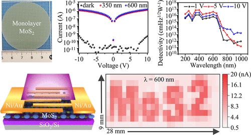
The discovery of an intrinsic direct bandgap in single-layer MoS2 has revealed significant potential for advancements in optoelectronic and photonic applications. This study aims to explore this potential by developing a high-performance Ni/Au metal–semiconductor–metal photodetector on wafer-scale epitaxially grown MoS2. The quality of the monolayer MoS2 film was verified using various techniques, including Raman, photoluminescence (PL), atomic force microscopy (AFM), X-ray photoelectron spectroscopy (XPS), and transmission electron microscopy (TEM). Results showed a high photoresponse of 2.06 and 0.68 A/W under 350 and 650 nm light illumination, respectively, at a 10 V reverse bias, along with an ultralow dark current measured in picoamps. These results indicate a low noise level and high photo-to-dark current rejection ratios of 5.45 × 10⁴ and 3.41 × 10⁴ under 350 and 650 nm illumination, respectively. The photodetector exhibited a maximum detectivity of 5.1 × 1016 cm Hz1/2 W–1 at 5 V under 350 nm of UV illumination, and the quantum efficiency surpassed 100% when the reverse bias voltage exceeded 3 V, demonstrating gain manifestation within the device. The dominance of a trap-assisted photoconductive gain mechanism was suggested by the power law exponent and the temporal characteristics observed. UV and visible imaging capabilities were also demonstrated using a “MoS2”-printed shadow mask and a single metal–semiconductor–metal (MSM) photodetector. This study highlights the superior photoimaging capabilities of the MoS2 MSM photodetector, offering substantial contributions to the field of optoelectronics and suggesting practical applications in photonic devices.
期刊介绍:
ACS Applied Materials & Interfaces is a leading interdisciplinary journal that brings together chemists, engineers, physicists, and biologists to explore the development and utilization of newly-discovered materials and interfacial processes for specific applications. Our journal has experienced remarkable growth since its establishment in 2009, both in terms of the number of articles published and the impact of the research showcased. We are proud to foster a truly global community, with the majority of published articles originating from outside the United States, reflecting the rapid growth of applied research worldwide.

 求助内容:
求助内容: 应助结果提醒方式:


