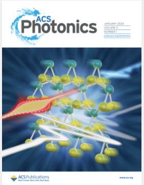
Ultrasensitive Pressure Sensing with Boron Vacancy Defects in Hexagonal Boron Nitride: In-Situ Pressure Imaging of Two-Dimensional Heterostructures under High Pressure
IF 6.5
1区 物理与天体物理
Q1 MATERIALS SCIENCE, MULTIDISCIPLINARY
引用次数: 0
Abstract
In-situ pressure imaging poses significant challenges due to strict experimental conditions. In this work, we integrate two-dimensional (2D) hexagonal boron nitride (hBN) with negative boron vacancy (VB–) spin defects directly into the chamber of the diamond anvil cell (DAC), enabling the first systematic investigation of their optical and spin properties under high pressure. Pressure-induced red-shifts of photoluminescence and reduced photon counts of the VB– defects are observed. The zero-field splitting parameter D of the VB– defects exhibits a linear pressure dependency at 57.4 MHz/GPa, with a pressure sensitivity of 0.32 , surpassing that of the nitrogen-vacancy centers in diamond and the silicon-vacancy centers in silicon carbon. Furthermore, by utilizing the VB– defects as ultrasensitive pressure quantum sensors, we have successfully mapped the inhomogeneous pressure distribution within an hBN/twisted double trilayer graphene/hBN device under compression via wide-field quantum imaging. The images reveal a pressure gradient increasing with loading. These results provide insight into the spin properties of VB– defects and the potential of in-situ pressure and magnetic imaging for 2D heterojunction devices under extreme conditions.

六方氮化硼中硼空位缺陷的超灵敏压力传感:高压下二维异质结构的原位压力成像
由于实验条件严格,现场压力成像面临着巨大的挑战。在这项工作中,我们将具有负硼空位(VB -)自旋缺陷的二维(2D)六方氮化硼(hBN)直接集成到金刚石砧细胞(DAC)的腔室中,从而首次系统地研究了它们在高压下的光学和自旋特性。观察到VB -缺陷的压力致发光红移和光子计数减少。在57.4 MHz/GPa时,VB -缺陷的零场分裂参数D与压力呈线性关系,压力灵敏度为0.32 MPa/Hz,超过了金刚石中的氮空位中心和硅碳中的硅空位中心。此外,利用VB -缺陷作为超灵敏的压力量子传感器,我们通过宽场量子成像成功地映射了hBN/扭曲双三层石墨烯/hBN器件在压缩下的非均匀压力分布。图像显示压力梯度随着载荷的增加而增加。这些结果揭示了VB -缺陷的自旋特性,以及在极端条件下二维异质结器件的原位压力和磁成像潜力。
本文章由计算机程序翻译,如有差异,请以英文原文为准。
求助全文
约1分钟内获得全文
求助全文
来源期刊

ACS Photonics
NANOSCIENCE & NANOTECHNOLOGY-MATERIALS SCIENCE, MULTIDISCIPLINARY
CiteScore
11.90
自引率
5.70%
发文量
438
审稿时长
2.3 months
期刊介绍:
Published as soon as accepted and summarized in monthly issues, ACS Photonics will publish Research Articles, Letters, Perspectives, and Reviews, to encompass the full scope of published research in this field.
 求助内容:
求助内容: 应助结果提醒方式:


