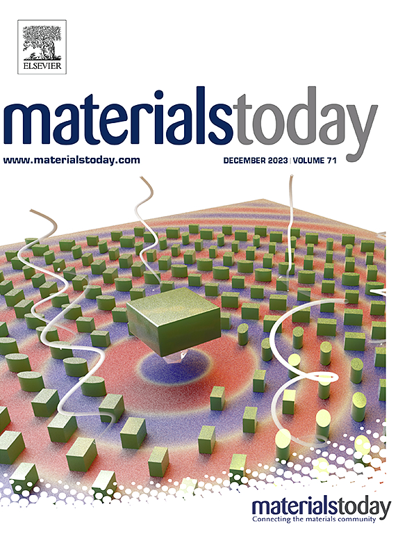
Defect-induced enhanced Raman scattering of two-dimensional materials
IF 21.1
1区 材料科学
Q1 MATERIALS SCIENCE, MULTIDISCIPLINARY
引用次数: 0
Abstract
Two-dimensional (2D) materials have emerged as compelling candidates for noble-metal-free surface-enhanced Raman scattering (SERS) substrates due to their atomic-scale thickness, tunable electronic properties, superior optical characteristics, and biocompatibility. While noble metal substrates rely on the electromagnetic mechanism (EM), defect engineering of 2D materials offers a transformative strategy to amplify their molecular sensing capabilities through the chemical mechanism (CM). This review article introduces defect-induced enhanced Raman scattering (DiERS) as a novel paradigm, where engineered defects in 2D materials—such as vacancies, dopants, grain boundaries, and heterostructures—precisely regulate charge transfer processes and molecular interactions. We systematically analyze defect generation methods across graphene and transition metal dichalcogenides (TMDCs), emphasizing scalable synthesis techniques (e.g., CVD, plasma etching) and advanced characterization tools (STEM, STM, CAFM) for atomic-level defect visualization. The core mechanisms of DiERS are elucidated through two critical pathways: (1) light-matter interactions, where defects modulate band structures to enhance resonant charge transfer, and (2) defect-matter interactions, involving defect-mediated adsorption and dipole effects that amplify molecular polarization. Furthermore, we highlight the potential applications of DiERS in ultrasensitive detection of environmental toxins (e.g., heavy metal ions, dyes), food contaminants (pesticides, additives), and biomedical diagnostics (neurotransmitters, viral proteins), achieving detection limits as low as 10-18 M. Challenges and future directions—including large-scale defect uniformity, standardized quantification protocols, and AI-driven spectral analysis—are discussed to advance DiERS toward next-generation molecular diagnostics and industrial scalability.

二维材料缺陷诱导的增强拉曼散射
二维(2D)材料由于其原子级厚度、可调谐电子特性、优越的光学特性和生物相容性,已成为无贵金属表面增强拉曼散射(SERS)衬底的引人注目的候选者。贵金属衬底依赖于电磁机制(EM),而二维材料的缺陷工程提供了一种通过化学机制(CM)增强其分子传感能力的变革策略。这篇综述文章介绍了缺陷诱导的增强拉曼散射(DiERS)作为一种新的范例,其中二维材料中的工程缺陷-如空位,掺杂剂,晶界和异质结构-精确地调节电荷转移过程和分子相互作用。我们系统地分析了石墨烯和过渡金属二硫化物(TMDCs)的缺陷生成方法,强调了可扩展的合成技术(例如,CVD,等离子体蚀刻)和先进的表征工具(STEM, STM, CAFM),用于原子水平的缺陷可视化。DiERS的核心机制是通过两个关键途径阐明的:(1)光-物质相互作用,缺陷调节能带结构以增强共振电荷转移;(2)缺陷-物质相互作用,包括缺陷介导的吸附和偶极子效应,放大分子极化。此外,我们强调了DiERS在超灵敏检测环境毒素(如重金属离子、染料)、食品污染物(农药、添加剂)和生物医学诊断(神经递质、病毒蛋白)方面的潜在应用,实现了低至10-18 m的检测限。挑战和未来的方向-包括大规模缺陷均匀性、标准化定量方案、以及人工智能驱动的光谱分析,以推动DiERS向下一代分子诊断和工业可扩展性发展。
本文章由计算机程序翻译,如有差异,请以英文原文为准。
求助全文
约1分钟内获得全文
求助全文
来源期刊

Materials Today
工程技术-材料科学:综合
CiteScore
36.30
自引率
1.20%
发文量
237
审稿时长
23 days
期刊介绍:
Materials Today is the leading journal in the Materials Today family, focusing on the latest and most impactful work in the materials science community. With a reputation for excellence in news and reviews, the journal has now expanded its coverage to include original research and aims to be at the forefront of the field.
We welcome comprehensive articles, short communications, and review articles from established leaders in the rapidly evolving fields of materials science and related disciplines. We strive to provide authors with rigorous peer review, fast publication, and maximum exposure for their work. While we only accept the most significant manuscripts, our speedy evaluation process ensures that there are no unnecessary publication delays.
 求助内容:
求助内容: 应助结果提醒方式:


