{"title":"Solution-Processed High-k BaTiO3 Nanocrystal Ultrathin Films as Insulators for Thin Film Transistors","authors":"Haowei Li, Dinghao Ma, Mengxin Liu, Xinan Shi*, Hao Huang* and Daocheng Pan*, ","doi":"10.1021/acsaelm.5c0054610.1021/acsaelm.5c00546","DOIUrl":null,"url":null,"abstract":"<p >The development of high-<i>k</i> and ultrathin gate insulators is critically important for advancing the miniaturization of field-effect transistors and realizing the “More than Moore” concept proposed by the IRDS. However, existing high-<i>k</i> gate insulators have yet to achieve an optimal balance among the thickness, band gap, breakdown strength, dielectric constant, and leakage current. In this study, oleic acid-capped BaTiO<sub>3</sub> (BTO) nanocrystals with an average size of 3.85 nm, which can be uniformly dispersed in toluene to form a highly transparent solution, are synthesized by a two-phase method. These nanocrystals form stable dispersion in toluene and enable spin-coating of uniform ultrathin (∼12 nm) films on silicon substrates. The resulting films exhibit a high dielectric constant (∼31), ultralow leakage current density (∼8.3 × 10<sup>–8</sup> A/cm<sup>2</sup> at 1 MV/cm), a capacitance equivalent thickness (CET) of 1.5 nm, and a breakdown field of 5 MV/cm. When used as the gate dielectric in fully inorganic thin-film transistors (TFTs) with CdS as the channel material, the BTO film yields <i>n</i>-channel device with a subthreshold swing (SS) as low as 70 mV/dec, a threshold voltage of 1.1 V, and an on/off ratio >10<sup>6</sup>. Integration with a monolayer MoS<sub>2</sub> channel produces TFT with an SS of 130 mV/dec and an on/off ratio >10<sup>5</sup>. These results underscore the potential of solution-processed BTO nanocrystalline films as high-performance gate dielectrics for next-generation nanoelectronics.</p>","PeriodicalId":3,"journal":{"name":"ACS Applied Electronic Materials","volume":"7 11","pages":"5126–5132 5126–5132"},"PeriodicalIF":4.7000,"publicationDate":"2025-05-21","publicationTypes":"Journal Article","fieldsOfStudy":null,"isOpenAccess":false,"openAccessPdf":"","citationCount":"0","resultStr":null,"platform":"Semanticscholar","paperid":null,"PeriodicalName":"ACS Applied Electronic Materials","FirstCategoryId":"88","ListUrlMain":"https://pubs.acs.org/doi/10.1021/acsaelm.5c00546","RegionNum":3,"RegionCategory":"材料科学","ArticlePicture":[],"TitleCN":null,"AbstractTextCN":null,"PMCID":null,"EPubDate":"","PubModel":"","JCR":"Q1","JCRName":"ENGINEERING, ELECTRICAL & ELECTRONIC","Score":null,"Total":0}
引用次数: 0
Abstract
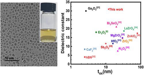
The development of high-k and ultrathin gate insulators is critically important for advancing the miniaturization of field-effect transistors and realizing the “More than Moore” concept proposed by the IRDS. However, existing high-k gate insulators have yet to achieve an optimal balance among the thickness, band gap, breakdown strength, dielectric constant, and leakage current. In this study, oleic acid-capped BaTiO3 (BTO) nanocrystals with an average size of 3.85 nm, which can be uniformly dispersed in toluene to form a highly transparent solution, are synthesized by a two-phase method. These nanocrystals form stable dispersion in toluene and enable spin-coating of uniform ultrathin (∼12 nm) films on silicon substrates. The resulting films exhibit a high dielectric constant (∼31), ultralow leakage current density (∼8.3 × 10⁻⁸ A/cm2 at 1 MV/cm), a capacitance equivalent thickness (CET) of 1.5 nm, and a breakdown field of 5 MV/cm. When used as the gate dielectric in fully inorganic thin-film transistors (TFTs) with CdS as the channel material, the BTO film yields n-channel device with a subthreshold swing (SS) as low as 70 mV/dec, a threshold voltage of 1.1 V, and an on/off ratio >106. Integration with a monolayer MoS2 channel produces TFT with an SS of 130 mV/dec and an on/off ratio >105. These results underscore the potential of solution-processed BTO nanocrystalline films as high-performance gate dielectrics for next-generation nanoelectronics.
期刊介绍:
ACS Applied Electronic Materials is an interdisciplinary journal publishing original research covering all aspects of electronic materials. The journal is devoted to reports of new and original experimental and theoretical research of an applied nature that integrate knowledge in the areas of materials science, engineering, optics, physics, and chemistry into important applications of electronic materials. Sample research topics that span the journal's scope are inorganic, organic, ionic and polymeric materials with properties that include conducting, semiconducting, superconducting, insulating, dielectric, magnetic, optoelectronic, piezoelectric, ferroelectric and thermoelectric.
Indexed/Abstracted:
Web of Science SCIE
Scopus
CAS
INSPEC
Portico

 求助内容:
求助内容: 应助结果提醒方式:


