Quasi-Homojunction Based on 1D-Chained Alloyed Sb2Se3 for High-Performance Broadband Photodetection and Matrix Imaging
IF 9.1
1区 材料科学
Q1 CHEMISTRY, MULTIDISCIPLINARY
引用次数: 0
Abstract
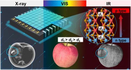
Junction-based photodiodes play a crucial role in integrated devices due to their compactness and efficient rectification. However, three-dimensional (3D) semiconductor heterojunctions suffer from high interface defects caused by lattice mismatch, while one-dimensional (1D) semiconductors feature large interchain gaps that alleviate lattice matching requirements and provide high strain relaxation, making them highly promising for homojunction construction. Herein, a quasi-homojunction is constructed via in situ Bi doping in 1D Sb2Se3. Compared to uniform film photodetectors, the quasi-homojunction-based photodetector exhibits a low dark current (4.8 nA cm–2), high light current (62.2 μA cm–2), high external quantum efficiency (35.5%@2.73 nW cm–2), and fast response speed. Furthermore, the photodetector is monolithically integrated on the thin-film transistor readout circuit for short-wavelength infrared imaging applications, demonstrated in a 64 × 64 pixel array. Moreover, the detectors exhibit a broadband detection from X-ray to near-infrared, showing potential application for image fusion. This work provides a novel strategy for broadband photodetectors and integration.
基于一维链化Sb2Se3的准同质结用于高性能宽带光探测和矩阵成像
基于结的光电二极管由于其紧凑和高效的整流而在集成器件中起着至关重要的作用。然而,三维(3D)半导体异质结存在由晶格失配引起的高界面缺陷,而一维(1D)半导体具有大的链间间隙,可以缓解晶格匹配要求并提供高应变松弛,使其在同质结构建中具有很高的前景。本文通过原位Bi掺杂在一维Sb2Se3中构建了准同质结。与均匀薄膜光电探测器相比,准同结光电探测器具有低暗电流(4.8 nA cm-2)、高光电流(62.2 μA cm-2)、高外量子效率(35.5%@2.73 nW cm-2)和快速响应的特点。此外,光电探测器单片集成在薄膜晶体管读出电路上,用于短波红外成像应用,以64 × 64像素阵列进行演示。此外,探测器表现出从x射线到近红外的宽带探测,显示出图像融合的潜在应用。这项工作为宽带光电探测器和集成提供了一种新的策略。
本文章由计算机程序翻译,如有差异,请以英文原文为准。
求助全文
约1分钟内获得全文
求助全文
来源期刊

Nano Letters
工程技术-材料科学:综合
CiteScore
16.80
自引率
2.80%
发文量
1182
审稿时长
1.4 months
期刊介绍:
Nano Letters serves as a dynamic platform for promptly disseminating original results in fundamental, applied, and emerging research across all facets of nanoscience and nanotechnology. A pivotal criterion for inclusion within Nano Letters is the convergence of at least two different areas or disciplines, ensuring a rich interdisciplinary scope. The journal is dedicated to fostering exploration in diverse areas, including:
- Experimental and theoretical findings on physical, chemical, and biological phenomena at the nanoscale
- Synthesis, characterization, and processing of organic, inorganic, polymer, and hybrid nanomaterials through physical, chemical, and biological methodologies
- Modeling and simulation of synthetic, assembly, and interaction processes
- Realization of integrated nanostructures and nano-engineered devices exhibiting advanced performance
- Applications of nanoscale materials in living and environmental systems
Nano Letters is committed to advancing and showcasing groundbreaking research that intersects various domains, fostering innovation and collaboration in the ever-evolving field of nanoscience and nanotechnology.
 求助内容:
求助内容: 应助结果提醒方式:


