112 Gb s−1 Germanium Photodetector at 2 µm Enabled by a 3D Integrated Waveguide Loop (Adv. Mater. Technol. 11/2025)
IF 6.4
3区 材料科学
Q1 MATERIALS SCIENCE, MULTIDISCIPLINARY
引用次数: 0
Abstract
Silicon Photonics
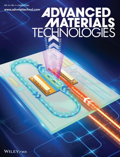
In article number 2401718, Jiangbing Du, Ke Xu, and co-workers show that an optical closed loop based on 3D integrated waveguides can be leveraged for enhanced light-matter interaction. The enhanced absorption enables high responsivity and large bandwidth for on-chip photodetectors beyond its cut-off wavelengths.


112 Gb s−1锗光电探测器,波长2µm,由3D集成波导环路(Adv. Mater.)实现。抛光工艺。11/2025)
在文章编号2401718中,杜江兵、徐珂及其同事展示了基于三维集成波导的光闭环可以用于增强光-物质相互作用。增强的吸收使片上光电探测器在其截止波长之外具有高响应性和大带宽。
本文章由计算机程序翻译,如有差异,请以英文原文为准。
求助全文
约1分钟内获得全文
求助全文
来源期刊
Advanced Materials Technologies
Materials Science-General Materials Science
CiteScore
10.20
自引率
4.40%
发文量
566
期刊介绍:
Advanced Materials Technologies Advanced Materials Technologies is the new home for all technology-related materials applications research, with particular focus on advanced device design, fabrication and integration, as well as new technologies based on novel materials. It bridges the gap between fundamental laboratory research and industry.
 求助内容:
求助内容: 应助结果提醒方式:


