Kimitaka Higuchi*, Tomoharu Tokunaga*, Toshiki Sato and Takahisa Yamamoto,
{"title":"Electron-Beam-Induced Crystallization of Amorphous Gallium Oxide Thin Films Using Scanning Transmission Electron Microscopy","authors":"Kimitaka Higuchi*, Tomoharu Tokunaga*, Toshiki Sato and Takahisa Yamamoto, ","doi":"10.1021/acs.cgd.5c0014810.1021/acs.cgd.5c00148","DOIUrl":null,"url":null,"abstract":"<p >Crystallization of amorphous materials using an electron beam is a promising technique for crystallizing minute regions. The crystallization behavior of amorphous gallium oxide (Ga<sub>2</sub>O<sub>3</sub>) thin films under electron-beam irradiation was investigated with a scanning transmission electron microscope, and patterned line drawing was performed using its line-scan mode. The Ga<sub>2</sub>O<sub>3</sub> thin films exhibited crystallization at threshold electron-beam doses in the range of 53–144 C/cm<sup>2</sup>. The γ- and β-Ga<sub>2</sub>O<sub>3</sub> forms crystallized as grains with an average size of 7 nm. The crystallization volume increased with doses. Crystallized Ga<sub>2</sub>O<sub>3</sub> polymorphs varied predominantly from γ- to β-Ga<sub>2</sub>O<sub>3</sub> with increased doses. The dose dependence of Ga<sub>2</sub>O<sub>3</sub> polymorphs was attributed to the variation in the coordination number of oxygen ions to gallium ions and the formation of oxygen vacancies caused by the electron-beam irradiation. The letter N predominantly composed of β-Ga<sub>2</sub>O<sub>3</sub> single crystals could be drawn with an approximately 10 nm line width in an amorphous Ga<sub>2</sub>O<sub>3</sub> thin film using the line-scan mode. Crystallized β-Ga<sub>2</sub>O<sub>3</sub> at the onset of the line-scan was inferred to grow epitaxially with subsequent scanning, realizing a letter N predominantly composed of single-crystal β-Ga<sub>2</sub>O<sub>3</sub>.</p>","PeriodicalId":34,"journal":{"name":"Crystal Growth & Design","volume":"25 11","pages":"3749–3755 3749–3755"},"PeriodicalIF":3.4000,"publicationDate":"2025-05-15","publicationTypes":"Journal Article","fieldsOfStudy":null,"isOpenAccess":false,"openAccessPdf":"","citationCount":"0","resultStr":null,"platform":"Semanticscholar","paperid":null,"PeriodicalName":"Crystal Growth & Design","FirstCategoryId":"92","ListUrlMain":"https://pubs.acs.org/doi/10.1021/acs.cgd.5c00148","RegionNum":2,"RegionCategory":"化学","ArticlePicture":[],"TitleCN":null,"AbstractTextCN":null,"PMCID":null,"EPubDate":"","PubModel":"","JCR":"Q2","JCRName":"CHEMISTRY, MULTIDISCIPLINARY","Score":null,"Total":0}
引用次数: 0
Abstract
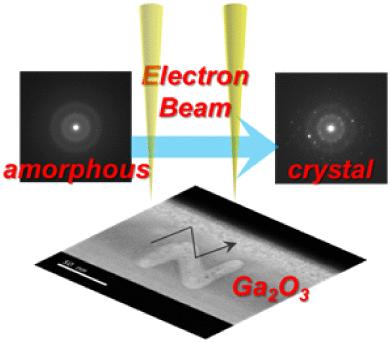
Crystallization of amorphous materials using an electron beam is a promising technique for crystallizing minute regions. The crystallization behavior of amorphous gallium oxide (Ga2O3) thin films under electron-beam irradiation was investigated with a scanning transmission electron microscope, and patterned line drawing was performed using its line-scan mode. The Ga2O3 thin films exhibited crystallization at threshold electron-beam doses in the range of 53–144 C/cm2. The γ- and β-Ga2O3 forms crystallized as grains with an average size of 7 nm. The crystallization volume increased with doses. Crystallized Ga2O3 polymorphs varied predominantly from γ- to β-Ga2O3 with increased doses. The dose dependence of Ga2O3 polymorphs was attributed to the variation in the coordination number of oxygen ions to gallium ions and the formation of oxygen vacancies caused by the electron-beam irradiation. The letter N predominantly composed of β-Ga2O3 single crystals could be drawn with an approximately 10 nm line width in an amorphous Ga2O3 thin film using the line-scan mode. Crystallized β-Ga2O3 at the onset of the line-scan was inferred to grow epitaxially with subsequent scanning, realizing a letter N predominantly composed of single-crystal β-Ga2O3.
期刊介绍:
The aim of Crystal Growth & Design is to stimulate crossfertilization of knowledge among scientists and engineers working in the fields of crystal growth, crystal engineering, and the industrial application of crystalline materials.
Crystal Growth & Design publishes theoretical and experimental studies of the physical, chemical, and biological phenomena and processes related to the design, growth, and application of crystalline materials. Synergistic approaches originating from different disciplines and technologies and integrating the fields of crystal growth, crystal engineering, intermolecular interactions, and industrial application are encouraged.

 求助内容:
求助内容: 应助结果提醒方式:


