Safdar Imam, Zhifu Liu, John A. Peters, Khasim Saheb Bayikadi, Pijush Bhattacharya and Mercouri G. Kanatzidis*,
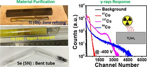
{"title":"Reducing Defect Density of Bridgman-Grown Tl6SeI4 Semiconductor Crystals for Room-Temperature γ-ray Detection","authors":"Safdar Imam, Zhifu Liu, John A. Peters, Khasim Saheb Bayikadi, Pijush Bhattacharya and Mercouri G. Kanatzidis*, ","doi":"10.1021/acs.cgd.5c0024210.1021/acs.cgd.5c00242","DOIUrl":null,"url":null,"abstract":"<p >The thallium-based halide semiconductor, Tl<sub>6</sub>SeI<sub>4</sub>, is a promising material for room-temperature X-ray and γ-ray detection; however, its performance has been limited by deep-level defects and thallium oxide impurities, which degrade charge transport and detection capabilities. In this study, we present an enhanced purification process for precursor materials (Tl, TlI, and Se) using zone refinement, vapor transport, and bent-tube techniques. This approach significantly reduces deep-level defects and impurities, enabling the growth of high-quality centimeter-sized Tl<sub>6</sub>SeI<sub>4</sub> single crystals using the two-zone vertical Bridgman method. Thermally stimulated current spectroscopy showed a reduction in defect density from ∼1.61 × 10<sup>15</sup> to ∼2.46 × 10<sup>13</sup> cm<sup>–3</sup>. The fabricated detectors exhibited high room-temperature resistivity (∼10<sup>10</sup> Ω·cm), effectively suppressing the leakage current. Improved photoresponses were observed for 122 keV γ-rays from <sup>57</sup>Co, 662 keV γ-rays from <sup>137</sup>Cs, and 1.173 MeV γ-rays from <sup>60</sup>Co, with particularly notable enhancements in detection efficiency for <sup>137</sup>Cs and <sup>60</sup>Co sources, compared to earlier studies with the same material. The mobility-lifetime (μτ) products were estimated to be 1.63 × 10<sup>–5</sup> cm<sup>2</sup>·V<sup>–1</sup> for electrons and 2.6 × 10<sup>–5</sup> cm<sup>2</sup>·V<sup>–1</sup> for holes, while time-of-flight measurements showed electron and hole drift mobilities of 26 and 18 cm<sup>2</sup>·V<sup>–1</sup>·s<sup>–1</sup>, respectively. These results highlight the critical importance of material purification in optimizing the Tl<sub>6</sub>SeI<sub>4</sub> detector performance.</p>","PeriodicalId":34,"journal":{"name":"Crystal Growth & Design","volume":"25 11","pages":"3826–3833 3826–3833"},"PeriodicalIF":3.4000,"publicationDate":"2025-05-21","publicationTypes":"Journal Article","fieldsOfStudy":null,"isOpenAccess":false,"openAccessPdf":"","citationCount":"0","resultStr":null,"platform":"Semanticscholar","paperid":null,"PeriodicalName":"Crystal Growth & Design","FirstCategoryId":"92","ListUrlMain":"https://pubs.acs.org/doi/10.1021/acs.cgd.5c00242","RegionNum":2,"RegionCategory":"化学","ArticlePicture":[],"TitleCN":null,"AbstractTextCN":null,"PMCID":null,"EPubDate":"","PubModel":"","JCR":"Q2","JCRName":"CHEMISTRY, MULTIDISCIPLINARY","Score":null,"Total":0}
引用次数: 0
Abstract
The thallium-based halide semiconductor, Tl6SeI4, is a promising material for room-temperature X-ray and γ-ray detection; however, its performance has been limited by deep-level defects and thallium oxide impurities, which degrade charge transport and detection capabilities. In this study, we present an enhanced purification process for precursor materials (Tl, TlI, and Se) using zone refinement, vapor transport, and bent-tube techniques. This approach significantly reduces deep-level defects and impurities, enabling the growth of high-quality centimeter-sized Tl6SeI4 single crystals using the two-zone vertical Bridgman method. Thermally stimulated current spectroscopy showed a reduction in defect density from ∼1.61 × 10¹⁵ to ∼2.46 × 1013 cm–3. The fabricated detectors exhibited high room-temperature resistivity (∼1010 Ω·cm), effectively suppressing the leakage current. Improved photoresponses were observed for 122 keV γ-rays from 57Co, 662 keV γ-rays from 137Cs, and 1.173 MeV γ-rays from 60Co, with particularly notable enhancements in detection efficiency for 137Cs and 60Co sources, compared to earlier studies with the same material. The mobility-lifetime (μτ) products were estimated to be 1.63 × 10⁻⁵ cm2·V–1 for electrons and 2.6 × 10⁻⁵ cm2·V–1 for holes, while time-of-flight measurements showed electron and hole drift mobilities of 26 and 18 cm2·V–1·s–1, respectively. These results highlight the critical importance of material purification in optimizing the Tl6SeI4 detector performance.
期刊介绍:
The aim of Crystal Growth & Design is to stimulate crossfertilization of knowledge among scientists and engineers working in the fields of crystal growth, crystal engineering, and the industrial application of crystalline materials.
Crystal Growth & Design publishes theoretical and experimental studies of the physical, chemical, and biological phenomena and processes related to the design, growth, and application of crystalline materials. Synergistic approaches originating from different disciplines and technologies and integrating the fields of crystal growth, crystal engineering, intermolecular interactions, and industrial application are encouraged.

 求助内容:
求助内容: 应助结果提醒方式:


