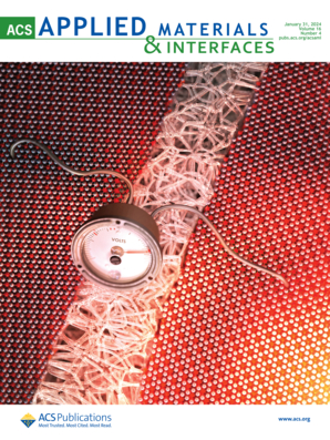
ALD-Grown ZnO TFTs Patterned by High-Resolution Reverse-Offset Printing
IF 8.3
2区 材料科学
Q1 MATERIALS SCIENCE, MULTIDISCIPLINARY
引用次数: 0
Abstract
Zinc oxide (ZnO) is a benign and earth-abundant semiconductor material that has been applied in thin-film transistors (TFTs) for decades and can be used in biodegradable, transient, and biocompatible devices. Printing as an alternative fabrication method to conventional TFT manufacturing methods can deliver some benefits, such as simultaneous film deposition and patterning, good scalability, low cost, and material-saving features. However, the high annealing temperature needed for ink-to-metal oxide conversion and film densification, compounded by the poor patterning resolution of conventional printing methods, still limits the use of printing in the fabrication of flexible metal oxide TFTs. Atomic layer deposition (ALD) has recently emerged as a promising fabrication method for high-performance metal oxide TFTs that can offer more conformal film growth, precise film thickness, and higher film quality at low temperatures compared to sputtering, spin coating, or printing. Although ALD-based ZnO TFTs patterned with photolithography exhibit good electrical properties, they cannot be readily scaled to a high-throughput fabrication. Very little attention has been paid so far to the combination of low-temperature ALD growth with printing to obtain more scalable manufacturing of high-performance thin-film electronics. To overcome this challenge, we propose high-resolution reverse-offset printing (ROP) of a simple polymer resist to pattern an ALD-grown ZnO film at few μm resolution to fabricate TFTs. In this work, we report high-performance ZnO TFTs that are ALD-grown at a low temperature of 150 °C and ROP-patterned with promising stability and uniformity, a high field-effect mobility (μFE) of ∼16.6 cm2 (Vs)−1, an almost zero turn-on voltage (Von) of ∼−0.49 V, a high current on–off ratio (Ion/Ioff) of >108, a low operation voltage (Vop) of ≤5 V, and a negligible hysteresis (Vhyst) of ∼0.13 V. The combination of ALD and the ROP-patterning process could be developed further to fabricate fully flexible high-resolution metal oxide TFT-based circuits in the future.

高解析度反胶印制备ZnO tft
氧化锌(ZnO)是一种良性且储量丰富的半导体材料,已应用于薄膜晶体管(TFTs)数十年,可用于生物可降解,瞬态和生物相容性器件。印刷作为传统TFT制造方法的替代制造方法可以提供一些好处,例如同时沉积薄膜和图案,良好的可扩展性,低成本和节省材料的特点。然而,油墨到金属氧化物转换和薄膜致密化所需的高退火温度,加上传统印刷方法的图案分辨率差,仍然限制了印刷在柔性金属氧化物tft制造中的使用。原子层沉积(ALD)最近成为高性能金属氧化物tft的一种有前途的制造方法,与溅射、自旋涂层或印刷相比,它可以在低温下提供更适形的薄膜生长、精确的薄膜厚度和更高的薄膜质量。虽然用光刻技术制作的基于ald的ZnO tft具有良好的电学性能,但它们不能很容易地扩展到高通量制造。到目前为止,很少有人关注低温ALD生长与印刷的结合,以获得更可扩展的高性能薄膜电子产品制造。为了克服这一挑战,我们提出了一种简单聚合物抗蚀剂的高分辨率反胶印(ROP),以在几μm分辨率下对ald生长的ZnO薄膜进行图案设计,以制造tft。在这项工作中,我们报道了在150°C低温下生长的高性能ZnO tft和rop模式,具有良好的稳定性和均匀性,高场效应迁移率(μFE)为~ 16.6 cm2 (Vs)−1,几乎为零的导通电压(Von)为~−0.49 V,高电流开关比(Ion/Ioff)为>;108,低工作电压(Vop)≤5 V,可忽略不计的迟滞(Vhyst)为~ 0.13 V。ALD和rop图像化工艺的结合可以在未来进一步发展,以制造全柔性高分辨率金属氧化物tft电路。
本文章由计算机程序翻译,如有差异,请以英文原文为准。
求助全文
约1分钟内获得全文
求助全文
来源期刊

ACS Applied Materials & Interfaces
工程技术-材料科学:综合
CiteScore
16.00
自引率
6.30%
发文量
4978
审稿时长
1.8 months
期刊介绍:
ACS Applied Materials & Interfaces is a leading interdisciplinary journal that brings together chemists, engineers, physicists, and biologists to explore the development and utilization of newly-discovered materials and interfacial processes for specific applications. Our journal has experienced remarkable growth since its establishment in 2009, both in terms of the number of articles published and the impact of the research showcased. We are proud to foster a truly global community, with the majority of published articles originating from outside the United States, reflecting the rapid growth of applied research worldwide.
 求助内容:
求助内容: 应助结果提醒方式:


