Capillary Epitaxy of Wide-Bandgap Copper Halide Single-Crystalline Film for Narrowband UV Photodetector and Dual-Mode Communication
IF 19
1区 材料科学
Q1 CHEMISTRY, MULTIDISCIPLINARY
引用次数: 0
Abstract
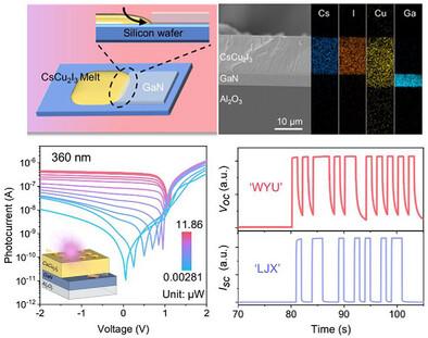
Wide-bandgap copper halide semiconductors hold significant potential for next-generation ultraviolet optoelectronics due to their remarkable photophysical properties. However, defects in polycrystalline films, such as point/interfacial defects and grain boundaries, create pathways for moisture and ion diffusion, thereby compromising device performance and stability. Herein, the capillary epitaxy growth of CsCu2I3 single-crystal films (SCFs) is demonstrated with a bandgap of 3.68 eV on GaN, by leveraging capillary forces to guide the transport of the molten precursor and using lattice-matching substrates to achieve crystallographic alignments. This strategy suppresses random nucleation and produces CsCu2I3 SCFs with high crystallinity (rocking curve FWHM = 0.286°). The critical role of lattice matching is further underscored by contrasting the polycrystalline CsCu2I3 or Cs3Cu2I5 films grown on lattice-mismatched substrates, as well as by the impressive open-circuit voltage of 1.08 V achieved in the CsCu2I3 SCF/GaN heterojunction. The CsCu2I3 SCF/GaN ultraviolet photodetectors demonstrate nW-level detection limit (≈2.81 nW) and self-powered operation, combining the 24 nm narrowband bandwidth with dual-mode (voltage/current) signal outputs for interference-resistant detection and communication. The work not only establishes the first route for the epitaxial growth of copper halide SCFs but also paves the way for the hetero-integration of perovskites onto mature semiconductor platforms for ultraviolet optoelectronics.
窄带紫外探测器和双模通信用宽带隙卤化铜单晶薄膜的毛细管外延
宽带隙卤化铜半导体由于其卓越的光物理特性,在下一代紫外光电子学中具有重要的潜力。然而,多晶薄膜中的缺陷,如点/界面缺陷和晶界,为水分和离子扩散创造了途径,从而影响了器件的性能和稳定性。本文通过利用毛细力引导熔融前驱体的输运,并使用晶格匹配衬底实现晶体排列,证明了ccu2i3单晶薄膜(SCFs)在GaN上的带隙为3.68 eV时的毛细外延生长。该策略抑制了随机成核,获得了高结晶度(摇摆曲线FWHM = 0.286°)的CsCu2I3 SCFs。通过对比在晶格不匹配的衬底上生长的多晶CsCu2I3或Cs3Cu2I5薄膜,以及在CsCu2I3 SCF/GaN异质结中获得的令人印象深刻的1.08 V开路电压,进一步强调了晶格匹配的关键作用。CsCu2I3 SCF/GaN紫外光电探测器具有nW级检测限(≈2.81 nW)和自供电功能,结合24 nm窄带带宽和双模(电压/电流)信号输出,可进行抗干扰检测和通信。这项工作不仅为卤化铜SCFs的外延生长建立了第一条途径,而且为钙钛矿在成熟的紫外光电子半导体平台上的异质集成铺平了道路。
本文章由计算机程序翻译,如有差异,请以英文原文为准。
求助全文
约1分钟内获得全文
求助全文
来源期刊
Advanced Functional Materials
工程技术-材料科学:综合
CiteScore
29.50
自引率
4.20%
发文量
2086
审稿时长
2.1 months
期刊介绍:
Firmly established as a top-tier materials science journal, Advanced Functional Materials reports breakthrough research in all aspects of materials science, including nanotechnology, chemistry, physics, and biology every week.
Advanced Functional Materials is known for its rapid and fair peer review, quality content, and high impact, making it the first choice of the international materials science community.
 求助内容:
求助内容: 应助结果提醒方式:


