Highly Efficient Planar Hot Electron Emitters Based on Ultrathin Pyrolyzed Polymer Films

IF 8.3 2区 材料科学 Q1 MATERIALS SCIENCE, MULTIDISCIPLINARY
Florian Herdl, Natalie Galfe, Sebastian Klenk, Michael Dillig, Silke Boche, Michael Bachmann, Andreas Schels, Simon Edler, Florian Dams, Andreas Pahlke, Georg S. Duesberg
{"title":"Highly Efficient Planar Hot Electron Emitters Based on Ultrathin Pyrolyzed Polymer Films","authors":"Florian Herdl, Natalie Galfe, Sebastian Klenk, Michael Dillig, Silke Boche, Michael Bachmann, Andreas Schels, Simon Edler, Florian Dams, Andreas Pahlke, Georg S. Duesberg","doi":"10.1021/acsami.4c19809","DOIUrl":null,"url":null,"abstract":"Miniaturized integrated hot electron emitters are highly sought after for application in chemical analytics and field-applicable systems. Here, we present the use of ultrathin pyrolyzed polymer films (PPFs) as the gate electrode, enabling the fabrication of highly efficient planar hot electron emitters (PHEEs). The thickness of the PPF was observed to be roughly 1 nm across a full 4” wafer, approaching the monolayer limit. Conductivities of up to 3.5 × 10<sup>4</sup> S/m at pyrolysis temperatures of only 900 °C were measured, representing a 2-fold increase compared to bulk values. This renders an easily accessible 2D material with high electron transparency. Thus, the PHEE exhibits very high transfer ratios of up to 31% and proves to be stable at high pressures over an extended period of time. Furthermore, the straightforward integration route of the PPF presented here comprises only two steps: photolithography and subsequent pyrolysis. The fabricated devices exhibit high uniformity in performance, with a transfer ratio standard deviation of 2.9% across a single wafer. Ultimately, the devices were fabricated exclusively with silicon dioxide on silicon in combination with carbon, which represents a sustainable fabrication approach with inert materials. It has been demonstrated that the PHEE can also operate in both nitrogen and air, illustrating the utility of these emitters for gas ionization and sensing.","PeriodicalId":5,"journal":{"name":"ACS Applied Materials & Interfaces","volume":"11 1","pages":""},"PeriodicalIF":8.3000,"publicationDate":"2025-05-30","publicationTypes":"Journal Article","fieldsOfStudy":null,"isOpenAccess":false,"openAccessPdf":"","citationCount":"0","resultStr":null,"platform":"Semanticscholar","paperid":null,"PeriodicalName":"ACS Applied Materials & Interfaces","FirstCategoryId":"88","ListUrlMain":"https://doi.org/10.1021/acsami.4c19809","RegionNum":2,"RegionCategory":"材料科学","ArticlePicture":[],"TitleCN":null,"AbstractTextCN":null,"PMCID":null,"EPubDate":"","PubModel":"","JCR":"Q1","JCRName":"MATERIALS SCIENCE, MULTIDISCIPLINARY","Score":null,"Total":0}
引用次数: 0

Abstract

Miniaturized integrated hot electron emitters are highly sought after for application in chemical analytics and field-applicable systems. Here, we present the use of ultrathin pyrolyzed polymer films (PPFs) as the gate electrode, enabling the fabrication of highly efficient planar hot electron emitters (PHEEs). The thickness of the PPF was observed to be roughly 1 nm across a full 4” wafer, approaching the monolayer limit. Conductivities of up to 3.5 × 10⁴ S/m at pyrolysis temperatures of only 900 °C were measured, representing a 2-fold increase compared to bulk values. This renders an easily accessible 2D material with high electron transparency. Thus, the PHEE exhibits very high transfer ratios of up to 31% and proves to be stable at high pressures over an extended period of time. Furthermore, the straightforward integration route of the PPF presented here comprises only two steps: photolithography and subsequent pyrolysis. The fabricated devices exhibit high uniformity in performance, with a transfer ratio standard deviation of 2.9% across a single wafer. Ultimately, the devices were fabricated exclusively with silicon dioxide on silicon in combination with carbon, which represents a sustainable fabrication approach with inert materials. It has been demonstrated that the PHEE can also operate in both nitrogen and air, illustrating the utility of these emitters for gas ionization and sensing.

Abstract Image

基于超薄热解聚合物薄膜的高效平面热电子发射体
小型化集成热电子发射器在化学分析和现场应用系统中备受追捧。在这里,我们提出使用超薄热解聚合物薄膜(PPFs)作为栅极,使高效率的平面热电子发射器(PHEEs)的制造成为可能。PPF的厚度在一整片4 "晶圆上约为1 nm,接近单层极限。在仅900℃的热解温度下,测量到的电导率高达3.5 × 10⁴ S/m,与散装值相比增加了2倍。这使得具有高电子透明度的二维材料易于获取。因此,PHEE表现出高达31%的高传递比,并在长时间的高压下保持稳定。此外,本文提出的PPF的直接集成路线只包括两个步骤:光刻和随后的热解。所制备的器件在性能上具有较高的均匀性,单晶圆上的传输比标准偏差为2.9%。最终,该装置完全由硅上的二氧化硅与碳结合而成,这代表了一种使用惰性材料的可持续制造方法。已经证明,PHEE也可以在氮气和空气中工作,说明这些发射器用于气体电离和传感的效用。
本文章由计算机程序翻译,如有差异,请以英文原文为准。
求助全文
约1分钟内获得全文 求助全文
来源期刊
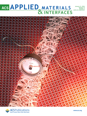
ACS Applied Materials & Interfaces
ACS Applied Materials & Interfaces 工程技术-材料科学:综合
CiteScore
16.00
自引率
6.30%
发文量
4978
审稿时长
1.8 months
期刊介绍: ACS Applied Materials & Interfaces is a leading interdisciplinary journal that brings together chemists, engineers, physicists, and biologists to explore the development and utilization of newly-discovered materials and interfacial processes for specific applications. Our journal has experienced remarkable growth since its establishment in 2009, both in terms of the number of articles published and the impact of the research showcased. We are proud to foster a truly global community, with the majority of published articles originating from outside the United States, reflecting the rapid growth of applied research worldwide.
×
引用
GB/T 7714-2015
复制
MLA
复制
APA
复制
导出至
BibTeX EndNote RefMan NoteFirst NoteExpress
×
提示
您的信息不完整,为了账户安全,请先补充。
现在去补充
×
提示
您因"违规操作"
具体请查看互助需知
我知道了
×
提示
确定
请完成安全验证×
copy
已复制链接
快去分享给好友吧!
我知道了
右上角分享
点击右上角分享
0
联系我们:info@booksci.cn Book学术提供免费学术资源搜索服务,方便国内外学者检索中英文文献。致力于提供最便捷和优质的服务体验。 Copyright © 2023 布克学术 All rights reserved.
京ICP备2023020795号-1
ghs 京公网安备 11010802042870号
Book学术文献互助
Book学术文献互助群
群 号:481959085
Book学术官方微信