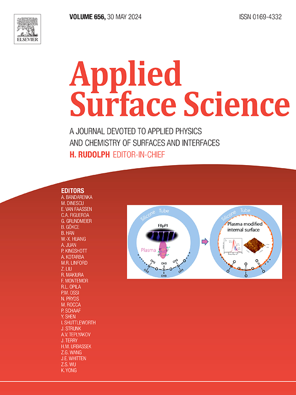
Tuning of solution-processed rGO-MoS2 bi-film transistor characteristics by selective layer nitrogen-doping
IF 6.3
2区 材料科学
Q2 CHEMISTRY, PHYSICAL
引用次数: 0
Abstract
A novel technique for depositing wafer-scale bi-films of graphene oxide (GO) and MoS2 with a thickness of 7 nm or less using the filter paper-assisted (FPA) method is present here. This method allows for the easy addition of a second layer without considering the nanosheet’s dimension or filter pore size. A GO density of 0.5 μg/cm2 exhibited single-layer coverage, where approximately a 6 nm MoS2 layer was deposited on GO. The resulting thin film was transferred onto a pre-patterned device. Reduced GO (rGO) and MoS2 layers were selectively treated with low-power ammonia plasma for nitrogen(N)-doping, followed by transistor channel preparation using photolithography and dry-etching techniques. The N-doping of rGO resulted in highly n-type transistor characteristics of the MoS2/rGO device prepared by the FPA method, improving electron mobility by 22.3 %. N-doping of MoS2 caused a p-type shift in the direct point (by 5.2 V) of the bi-film device. Both the FPA thin film and the prepared devices displayed uniform characteristics across the wafer, indicating the scalability and uniformity achieved by the proposed FPA method.

选择性氮层掺杂对溶液制rGO-MoS2双膜晶体管特性的调节
本文提出了一种利用滤纸辅助(FPA)方法沉积厚度为7 nm或更小的氧化石墨烯(GO)和MoS2的晶圆级双膜的新技术。这种方法可以很容易地添加第二层,而无需考虑纳米片的尺寸或过滤器的孔径。当氧化石墨烯密度为0.5 μg/cm2时,氧化石墨烯呈现单层覆盖,其中约有6 nm的MoS2层沉积在氧化石墨烯上。所得到的薄膜被转移到一个预图案化的装置上。采用低功率氨等离子体对还原氧化石墨烯(rGO)和MoS2层进行选择性氮掺杂处理,然后采用光刻和干蚀刻技术制备晶体管通道。rGO的n掺杂使得FPA法制备的MoS2/rGO器件具有高n型晶体管特性,电子迁移率提高了22.3% %。MoS2的n掺杂引起双膜器件直接点的p型位移(5.2 V)。所制备的FPA薄膜和器件在整个晶圆上都显示出均匀的特性,表明所提出的FPA方法实现了可扩展性和均匀性。
本文章由计算机程序翻译,如有差异,请以英文原文为准。
求助全文
约1分钟内获得全文
求助全文
来源期刊

Applied Surface Science
工程技术-材料科学:膜
CiteScore
12.50
自引率
7.50%
发文量
3393
审稿时长
67 days
期刊介绍:
Applied Surface Science covers topics contributing to a better understanding of surfaces, interfaces, nanostructures and their applications. The journal is concerned with scientific research on the atomic and molecular level of material properties determined with specific surface analytical techniques and/or computational methods, as well as the processing of such structures.
 求助内容:
求助内容: 应助结果提醒方式:


