{"title":"A local de-insulation method and its application in neural microneedle array.","authors":"Xin Zhao, Chunrong Wei, Deguang Zhu, Xiaowei Yang, Guowei Han, Jin Ning, Qiang Gui, Rongyu Tang, Yijun Wang, Jingfeng Zhou, Zhaoxin Geng, Weihua Pei","doi":"10.1038/s41378-025-00922-6","DOIUrl":null,"url":null,"abstract":"<p><p>Silicon-based neural microneedle arrays, such as the Utah Array, have demonstrated excellent performance in chronic recordings from the cerebral cortex. Unlike planar thin-film electrodes with recording sites arranged on the surface of a silicon film, the recording sites of microneedle arrays are located at the tips of three-dimensional needles, which significantly complicates the fabrication process required for single-neuron recordings. To address this challenge, we develop a local de-insulation method for microneedle recording electrodes that eliminates the need for etching: the microneedle tips are encapsulated in a controllable-thickness protective layer, followed by deposition of a Parylene-C insulation layer. By optimizing the elasticity of the protection material, as well as its adhesion and shape on both the protective layer and the electrode shaft, we were able to precisely control the area of the removed insulated layers, resulting in consistent tip exposure. Experimental results show that the non-uniformity of the exposed microneedle recording sites in the silicon-based neural microelectrode arrays (each has 10 × 10 array) fabricated using this method is 3.32 ± 1.02%. Furthermore, the arrays exhibited high stability and reliability in both mechanical performance and electrical characteristics. They achieved an average spike signal-to-noise ratio of 12.63 ± 6.64 during in vivo testing. This fabrication technique provides a valuable method for the development of high-performance neural microelectrode array.</p>","PeriodicalId":18560,"journal":{"name":"Microsystems & Nanoengineering","volume":"11 1","pages":"103"},"PeriodicalIF":9.9000,"publicationDate":"2025-05-26","publicationTypes":"Journal Article","fieldsOfStudy":null,"isOpenAccess":false,"openAccessPdf":"https://www.ncbi.nlm.nih.gov/pmc/articles/PMC12106818/pdf/","citationCount":"0","resultStr":null,"platform":"Semanticscholar","paperid":null,"PeriodicalName":"Microsystems & Nanoengineering","FirstCategoryId":"5","ListUrlMain":"https://doi.org/10.1038/s41378-025-00922-6","RegionNum":1,"RegionCategory":"工程技术","ArticlePicture":[],"TitleCN":null,"AbstractTextCN":null,"PMCID":null,"EPubDate":"","PubModel":"","JCR":"Q1","JCRName":"INSTRUMENTS & INSTRUMENTATION","Score":null,"Total":0}
引用次数: 0
Abstract
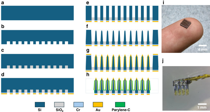
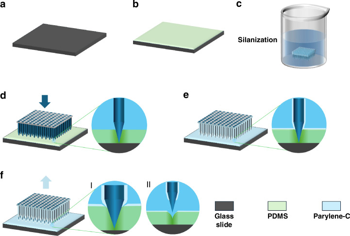
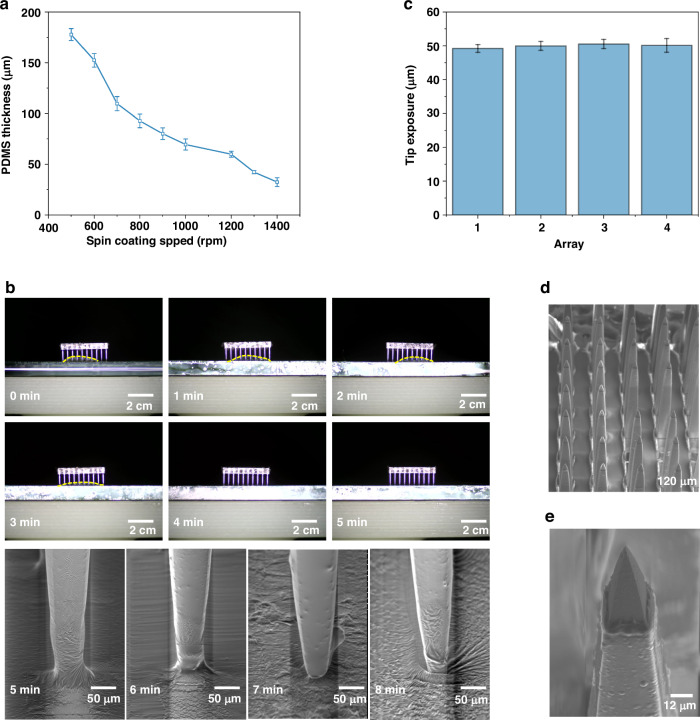
Silicon-based neural microneedle arrays, such as the Utah Array, have demonstrated excellent performance in chronic recordings from the cerebral cortex. Unlike planar thin-film electrodes with recording sites arranged on the surface of a silicon film, the recording sites of microneedle arrays are located at the tips of three-dimensional needles, which significantly complicates the fabrication process required for single-neuron recordings. To address this challenge, we develop a local de-insulation method for microneedle recording electrodes that eliminates the need for etching: the microneedle tips are encapsulated in a controllable-thickness protective layer, followed by deposition of a Parylene-C insulation layer. By optimizing the elasticity of the protection material, as well as its adhesion and shape on both the protective layer and the electrode shaft, we were able to precisely control the area of the removed insulated layers, resulting in consistent tip exposure. Experimental results show that the non-uniformity of the exposed microneedle recording sites in the silicon-based neural microelectrode arrays (each has 10 × 10 array) fabricated using this method is 3.32 ± 1.02%. Furthermore, the arrays exhibited high stability and reliability in both mechanical performance and electrical characteristics. They achieved an average spike signal-to-noise ratio of 12.63 ± 6.64 during in vivo testing. This fabrication technique provides a valuable method for the development of high-performance neural microelectrode array.
期刊介绍:
Microsystems & Nanoengineering is a comprehensive online journal that focuses on the field of Micro and Nano Electro Mechanical Systems (MEMS and NEMS). It provides a platform for researchers to share their original research findings and review articles in this area. The journal covers a wide range of topics, from fundamental research to practical applications. Published by Springer Nature, in collaboration with the Aerospace Information Research Institute, Chinese Academy of Sciences, and with the support of the State Key Laboratory of Transducer Technology, it is an esteemed publication in the field. As an open access journal, it offers free access to its content, allowing readers from around the world to benefit from the latest developments in MEMS and NEMS.
 求助内容:
求助内容: 应助结果提醒方式:


