Comprehensive analysis and investigation of GaN LNA for 3–4 GHz using different gate-drain spacing
IF 3.1
4区 工程技术
Q2 ENGINEERING, ELECTRICAL & ELECTRONIC
引用次数: 0
Abstract
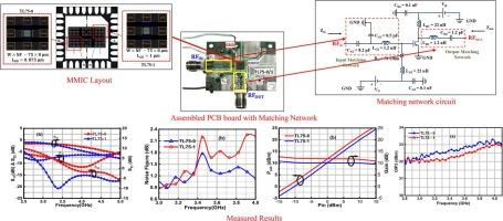
This work investigates the impact of the device technological parameter - gate-drain access region spacing () - for GaN High Electron Mobility Transistors (HEMTs), on the design of low noise amplifiers (LNAs) for the 3–4 GHz range. We compare two GaN LNA variants, characterized by values of and , to highlight the significance of gate-drain spacings in determining performance metrics. This study contributes insights into the effect of gate-drain spacing on the GaN LNAs, and evaluates the RF characteristics, Noise Fig. (NF), and power metrics for different values. Based on our findings, we assert that the LNA exhibits superior performance over its counterpart in the evaluated benchmarks, along with the physical reasoning.
不同栅极-漏极间距下3 - 4ghz GaN LNA的综合分析与研究
本研究探讨了氮化镓高电子迁移率晶体管(hemt)的器件技术参数-栅极-漏极通路区域间距(LGD)对3-4 GHz范围内低噪声放大器(lna)设计的影响。我们比较了两种GaN LNA变体,其LGD值分别为0.875μm和1μm,以强调栅极漏极间距在决定性能指标中的重要性。本研究深入探讨了栅极-漏极间距对GaN LNAs的影响,并评估了不同LGD值下的射频特性、噪声图(NF)和功率指标。基于我们的研究结果,我们断言0.875μmLGD LNA在评估基准中表现出优于其对应的性能,以及物理推理。
本文章由计算机程序翻译,如有差异,请以英文原文为准。
求助全文
约1分钟内获得全文
求助全文
来源期刊

Microelectronic Engineering
工程技术-工程:电子与电气
CiteScore
5.30
自引率
4.30%
发文量
131
审稿时长
29 days
期刊介绍:
Microelectronic Engineering is the premier nanoprocessing, and nanotechnology journal focusing on fabrication of electronic, photonic, bioelectronic, electromechanic and fluidic devices and systems, and their applications in the broad areas of electronics, photonics, energy, life sciences, and environment. It covers also the expanding interdisciplinary field of "more than Moore" and "beyond Moore" integrated nanoelectronics / photonics and micro-/nano-/bio-systems. Through its unique mixture of peer-reviewed articles, reviews, accelerated publications, short and Technical notes, and the latest research news on key developments, Microelectronic Engineering provides comprehensive coverage of this exciting, interdisciplinary and dynamic new field for researchers in academia and professionals in industry.
 求助内容:
求助内容: 应助结果提醒方式:


