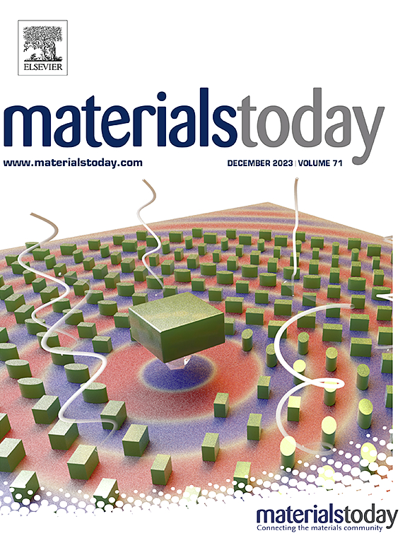
Ultra-fast on-chip VUV (λ<200 nm) photodiode integration
IF 21.1
1区 材料科学
Q1 MATERIALS SCIENCE, MULTIDISCIPLINARY
引用次数: 0
Abstract
In the fields of biomedicine and integrated circuits, the understanding of structural functions on the nanoscale is of great significance. However, when the size is smaller than 100 nm, the visible light cannot directly detect the structure at this scale. According to Ruili judgment, vacuum ultraviolet (VUV, 10–200 nm) can provide a channel for structural representation and imaging when the scale is smaller than 100 nm. Therefore, the use of high-space-resolution VUV microscopes can realize the device structure representation on the nanoscale. One of the vital compositions in high-space-resolution VUV microscopes is the VUV photodetector with imaging capabilities. Current commercial silicon-based imaging detectors have the disadvantage of broad spectral response. Here, an on-chip VUV photodiode integration with a vertical structure of Pt/AlN/n-Si heterojunctions was constructed on high-quality AlN thin films based on n-Si substrates using the MOCVD method, exhibiting photovoltaic responsivity and high integration. The device has an ultra-high light-to-dark ratio (∼107), ultra-fast photoresponse (τr ∼ 12.4 ns, τd ∼ 49.6 ns) and high response rate (52.23 mA/W). Impressively, each array has a high degree of uniformity, reproducibility, and stability. In addition, the device can accurately detect the English letters “F” and “T”. This work not only benefits the high integration of VUV imaging sensors but also provides a new research idea for next-generation VUV microscopes with high spatial resolution.

超高速片上VUV (λ< 200nm)光电二极管集成
在生物医学和集成电路领域,对纳米尺度结构功能的理解具有重要意义。然而,当尺寸小于100 nm时,可见光无法直接探测到该尺度的结构。根据瑞丽的判断,当尺度小于100 nm时,真空紫外(VUV, 10-200 nm)可以为结构表征和成像提供通道。因此,利用高空间分辨率的紫外显微镜可以实现纳米尺度上的器件结构表征。具有成像能力的紫外光电探测器是高空间分辨率紫外显微镜的重要组成部分之一。目前商用硅基成像探测器存在光谱响应较宽的缺点。本文采用MOCVD方法,在基于n-Si衬底的高质量AlN薄膜上构建了具有Pt/AlN/n-Si异质结垂直结构的片上VUV光电二极管,具有光伏响应性和高集成度。该器件具有超高的光暗比(~ 107),超快的光响应(τr ~ 12.4 ns, τd ~ 49.6 ns)和高响应率(52.23 mA/W)。令人印象深刻的是,每个阵列都具有高度的均匀性、再现性和稳定性。此外,该设备还能准确检测英文字母“F”和“T”。这项工作不仅有利于VUV成像传感器的高集成度,而且为下一代高空间分辨率VUV显微镜的研究提供了新的思路。
本文章由计算机程序翻译,如有差异,请以英文原文为准。
求助全文
约1分钟内获得全文
求助全文
来源期刊

Materials Today
工程技术-材料科学:综合
CiteScore
36.30
自引率
1.20%
发文量
237
审稿时长
23 days
期刊介绍:
Materials Today is the leading journal in the Materials Today family, focusing on the latest and most impactful work in the materials science community. With a reputation for excellence in news and reviews, the journal has now expanded its coverage to include original research and aims to be at the forefront of the field.
We welcome comprehensive articles, short communications, and review articles from established leaders in the rapidly evolving fields of materials science and related disciplines. We strive to provide authors with rigorous peer review, fast publication, and maximum exposure for their work. While we only accept the most significant manuscripts, our speedy evaluation process ensures that there are no unnecessary publication delays.
 求助内容:
求助内容: 应助结果提醒方式:


