D Panna, R Itzhak, A Kumar, S Bouscher, N Suleymanov, B Minkovich, Z Gan, A George, A Turchanin, I Goykhman, A Hayat
{"title":"Andreev pair injection into a transition metal dichalcogenide monolayer.","authors":"D Panna, R Itzhak, A Kumar, S Bouscher, N Suleymanov, B Minkovich, Z Gan, A George, A Turchanin, I Goykhman, A Hayat","doi":"10.1038/s41699-025-00553-5","DOIUrl":null,"url":null,"abstract":"<p><p>We demonstrate Andreev pair injection across Nb-WS<sub>2</sub> junction evident as Andreev reflection in differential conductivity spectra below Nb critical temperature <math> <msub><mrow><mi>T</mi></mrow> <mrow><mi>c</mi></mrow> </msub> </math> . The superconducting- 2D semiconducting junction defined by a focused ion beam, shaped Nb pads, and semi-dry transfer of single layer CVD-grown WS<sub>2</sub> crystals ensured the mechanical integrity of the 2D TMD film, reduced contamination and defects at Nb-WS<sub>2</sub> junction, enabling the pristine study of the interface and facilitating Andreev pair injection. We observed enhanced conductivity in <math><mrow><mi>dI</mi> <mo>/</mo> <mi>dV</mi></mrow> </math> spectra for junction voltages smaller than the corresponding Nb superconducting gap, which vanishes as the device temperature is increased above the <math> <msub><mrow><mi>T</mi></mrow> <mrow><mi>c</mi></mrow> </msub> </math> . The position and the temperature dependence of the conductivity peaks suggest proximity effect-related phenomena explained by developed modified BTK theory. The presented results are crucial for the future implementation of proximity-based 2D hybrid devices including quantum light sources and superconducting field-effect transistors based on superconductor-semiconductor junctions.</p>","PeriodicalId":19227,"journal":{"name":"npj 2D Materials and Applications","volume":"9 1","pages":"36"},"PeriodicalIF":8.8000,"publicationDate":"2025-01-01","publicationTypes":"Journal Article","fieldsOfStudy":null,"isOpenAccess":false,"openAccessPdf":"https://www.ncbi.nlm.nih.gov/pmc/articles/PMC12049272/pdf/","citationCount":"0","resultStr":null,"platform":"Semanticscholar","paperid":null,"PeriodicalName":"npj 2D Materials and Applications","FirstCategoryId":"88","ListUrlMain":"https://doi.org/10.1038/s41699-025-00553-5","RegionNum":2,"RegionCategory":"材料科学","ArticlePicture":[],"TitleCN":null,"AbstractTextCN":null,"PMCID":null,"EPubDate":"2025/5/3 0:00:00","PubModel":"Epub","JCR":"Q1","JCRName":"MATERIALS SCIENCE, MULTIDISCIPLINARY","Score":null,"Total":0}
引用次数: 0
Abstract
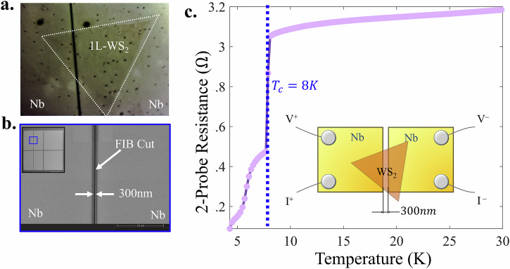
We demonstrate Andreev pair injection across Nb-WS2 junction evident as Andreev reflection in differential conductivity spectra below Nb critical temperature . The superconducting- 2D semiconducting junction defined by a focused ion beam, shaped Nb pads, and semi-dry transfer of single layer CVD-grown WS2 crystals ensured the mechanical integrity of the 2D TMD film, reduced contamination and defects at Nb-WS2 junction, enabling the pristine study of the interface and facilitating Andreev pair injection. We observed enhanced conductivity in spectra for junction voltages smaller than the corresponding Nb superconducting gap, which vanishes as the device temperature is increased above the . The position and the temperature dependence of the conductivity peaks suggest proximity effect-related phenomena explained by developed modified BTK theory. The presented results are crucial for the future implementation of proximity-based 2D hybrid devices including quantum light sources and superconducting field-effect transistors based on superconductor-semiconductor junctions.
期刊介绍:
npj 2D Materials and Applications publishes papers on the fundamental behavior, synthesis, properties and applications of existing and emerging 2D materials. By selecting papers with the potential for impact, the journal aims to facilitate the transfer of the research of 2D materials into wide-ranging applications.
 求助内容:
求助内容: 应助结果提醒方式:


