Direct Visualization of Metal-Induced Gap State Distribution and Valley Band Evolution at Metal Versus Semimetal MoS2 Interfaces
IF 16
1区 材料科学
Q1 CHEMISTRY, MULTIDISCIPLINARY
引用次数: 0
Abstract
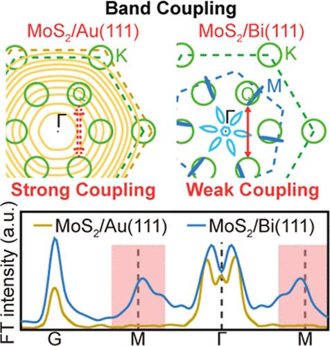
The interlayer coupling between metals and the two-dimensional (2D) semiconductors’ conduction band (CB), encompassing metal-induced gap states (MIGS) and valley band modulation, critically influences both the Schottky barrier height (SBH) and intrinsic sheet resistance. Understanding the CB modulation induced by metals/semimetals is, therefore, essential for contact engineering optimization. Given that the MIGS decay length and orbital interactions are spatially confined to the nanoscale region proximate to the 2D semiconductor interface, we employed scanning tunneling microscopy/spectroscopy to quantitatively determine the MIGS decay length and CB minimum on various metal/semimetal substrates. This approach enabled the comprehensive characterization of MIGS distribution, charge neutrality level variation, and SBH properties. Our findings demonstrate that maintaining valley band structure integrity during semimetal interlayer coupling facilitates reduced intrinsic sheet resistance. These results elucidate the mechanism underlying weak interlayer coupling at semimetal–2D semiconductor junctions and their superior contact transport performance, providing insights into the rational design of future 2D-based devices.
金属与半金属MoS2界面上金属诱导的隙态分布和谷带演化的直接可视化
金属与二维(2D)半导体导带(CB)之间的层间耦合,包括金属诱导的间隙态(MIGS)和谷带调制,严重影响肖特基势垒高度(SBH)和固有片电阻。因此,了解金属/半金属引起的CB调制对于接触工程优化至关重要。考虑到MIGS衰变长度和轨道相互作用在空间上局限于接近二维半导体界面的纳米级区域,我们使用扫描隧道显微镜/光谱法定量确定了各种金属/半金属衬底上的MIGS衰变长度和最小CB值。这种方法能够全面表征MIGS分布、电荷中性能级变化和SBH特性。我们的研究结果表明,在半金属层间耦合过程中保持谷带结构的完整性有助于降低固有的薄片电阻。这些结果阐明了半金属- 2d半导体结弱层间耦合的机制及其优越的接触传输性能,为未来基于2d的器件的合理设计提供了见解。
本文章由计算机程序翻译,如有差异,请以英文原文为准。
求助全文
约1分钟内获得全文
求助全文
来源期刊

ACS Nano
工程技术-材料科学:综合
CiteScore
26.00
自引率
4.10%
发文量
1627
审稿时长
1.7 months
期刊介绍:
ACS Nano, published monthly, serves as an international forum for comprehensive articles on nanoscience and nanotechnology research at the intersections of chemistry, biology, materials science, physics, and engineering. The journal fosters communication among scientists in these communities, facilitating collaboration, new research opportunities, and advancements through discoveries. ACS Nano covers synthesis, assembly, characterization, theory, and simulation of nanostructures, nanobiotechnology, nanofabrication, methods and tools for nanoscience and nanotechnology, and self- and directed-assembly. Alongside original research articles, it offers thorough reviews, perspectives on cutting-edge research, and discussions envisioning the future of nanoscience and nanotechnology.
 求助内容:
求助内容: 应助结果提醒方式:


