Channel and contact length scaling of two-dimensional transistors using composite metal electrodes
IF 40.9
1区 工程技术
Q1 ENGINEERING, ELECTRICAL & ELECTRONIC
引用次数: 0
Abstract
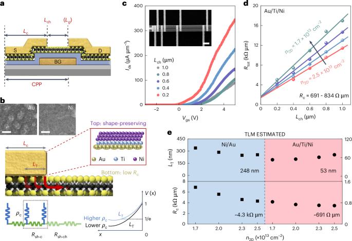
Two-dimensional semiconductors are a potential channel material for transistors with highly scaled contacted poly pitch (CPP). Total scaling of CPP requires the simultaneous reduction of channel length and contact length. However, the physical width limit of contact metals makes it difficult to form effective small-size contacts. In addition, decreasing the contact length below the transfer length induces a current crowding phenomenon, resulting in an exponential increase in contact resistance and poor device performance. Here we show that composite metal contact electrodes of gold/titanium/nickel can offer shape-preserving effects that allow the extreme scaling of contact length in two-dimensional transistors while maintaining a low contact resistance. We use the approach to create molybdenum disulfide transistors with a CPP of around 60 nm—contact length and channel length scaled to around 30 nm and transfer length scaled to under 30 nm—that exhibit on/off ratios over 108, on-state currents of around 300 μA μm−1 and off-state currents down to around 1 pA μm−1. We also fabricate arrays of all-out scaled two-dimensional transistors that exhibit low variability in key performance metrics and demonstrate their integration into advanced logic circuits. The channel and contact lengths of monolayer molybdenum disulfide field-effect transistors can be scaled to 30 nm using metal composite contacts that reduce the current crowding phenomenon.

利用复合金属电极的二维晶体管沟道和接触长度缩放
二维半导体是高尺度接触多间距(CPP)晶体管的潜在沟道材料。CPP的总缩放要求同时减少通道长度和接触长度。然而,接触金属的物理宽度限制使得难以形成有效的小尺寸接触。此外,当接触长度小于传递长度时,会产生电流拥挤现象,导致接触电阻呈指数增长,器件性能变差。在这里,我们展示了金/钛/镍的复合金属接触电极可以提供形状保持效果,允许在保持低接触电阻的同时在二维晶体管中极端缩放接触长度。我们使用该方法制造出CPP约为60 nm的二硫化钼晶体管,其接触长度和通道长度缩放到约30 nm,转移长度缩放到30 nm以下,其开/关比超过108,导通电流约为300 μA μm−1,关断电流约为1 pA μm−1。我们还制造了全面缩放的二维晶体管阵列,这些晶体管在关键性能指标上表现出低可变性,并展示了它们与高级逻辑电路的集成。
本文章由计算机程序翻译,如有差异,请以英文原文为准。
求助全文
约1分钟内获得全文
求助全文
来源期刊
Nature Electronics
Engineering-Electrical and Electronic Engineering
CiteScore
47.50
自引率
2.30%
发文量
159
期刊介绍:
Nature Electronics is a comprehensive journal that publishes both fundamental and applied research in the field of electronics. It encompasses a wide range of topics, including the study of new phenomena and devices, the design and construction of electronic circuits, and the practical applications of electronics. In addition, the journal explores the commercial and industrial aspects of electronics research.
The primary focus of Nature Electronics is on the development of technology and its potential impact on society. The journal incorporates the contributions of scientists, engineers, and industry professionals, offering a platform for their research findings. Moreover, Nature Electronics provides insightful commentary, thorough reviews, and analysis of the key issues that shape the field, as well as the technologies that are reshaping society.
Like all journals within the prestigious Nature brand, Nature Electronics upholds the highest standards of quality. It maintains a dedicated team of professional editors and follows a fair and rigorous peer-review process. The journal also ensures impeccable copy-editing and production, enabling swift publication. Additionally, Nature Electronics prides itself on its editorial independence, ensuring unbiased and impartial reporting.
In summary, Nature Electronics is a leading journal that publishes cutting-edge research in electronics. With its multidisciplinary approach and commitment to excellence, the journal serves as a valuable resource for scientists, engineers, and industry professionals seeking to stay at the forefront of advancements in the field.
 求助内容:
求助内容: 应助结果提醒方式:


