Zhenyuan Tang, Fu Li, Miao Peng, Wenke Fu, Xia Liu, Jingyuan Zhang, Guanghai Fei and Min Tu*,
{"title":"Wafer-Scale Integration of Metal Oxide Nanocrystals on Gas Sensor Chips via Direct Lithographic Patterning","authors":"Zhenyuan Tang, Fu Li, Miao Peng, Wenke Fu, Xia Liu, Jingyuan Zhang, Guanghai Fei and Min Tu*, ","doi":"10.1021/acssensors.4c03663","DOIUrl":null,"url":null,"abstract":"<p >Nanomaterial-based gas sensors are essential due to their high sensitivity and scalability, enabling efficient gas detection across diverse applications. However, a key challenge hindering their practical applications is the variation in sensing performance between devices. Addressing this requires careful consideration of the relationship between on-chip sensing materials and miniaturized devices. As feature sizes reduce to the microscale, accurately and uniformly positioning sensing nanomaterials onto specific regions of the device electrodes becomes increasingly difficult. This challenge arises from the incompatibility between the bottom-up nanomaterial synthesis methods and the top-down lithography-based fabrication processes. Herein, we introduce a cleanroom-compatible fabrication workflow for chemiresistive gas sensors employing direct lithographic patterning of metal oxide nanocrystals. Gas sensors located across different regions of a 4 in. wafer exhibit highly consistent gas-sensing performances, highlighting the potential of this approach, which integrates the strengths of both top-down and bottom-up approaches. This approach opens new opportunities for integrating a wide range of bottom-up synthesized functional nanomaterials into diverse types of chemical sensors.</p>","PeriodicalId":24,"journal":{"name":"ACS Sensors","volume":"10 8","pages":"5520–5527"},"PeriodicalIF":9.1000,"publicationDate":"2025-05-06","publicationTypes":"Journal Article","fieldsOfStudy":null,"isOpenAccess":false,"openAccessPdf":"","citationCount":"0","resultStr":null,"platform":"Semanticscholar","paperid":null,"PeriodicalName":"ACS Sensors","FirstCategoryId":"92","ListUrlMain":"https://pubs.acs.org/doi/10.1021/acssensors.4c03663","RegionNum":1,"RegionCategory":"化学","ArticlePicture":[],"TitleCN":null,"AbstractTextCN":null,"PMCID":null,"EPubDate":"","PubModel":"","JCR":"Q1","JCRName":"CHEMISTRY, ANALYTICAL","Score":null,"Total":0}
引用次数: 0
Abstract
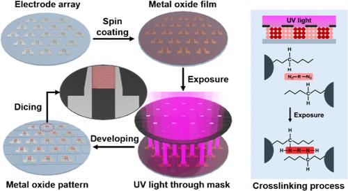
Nanomaterial-based gas sensors are essential due to their high sensitivity and scalability, enabling efficient gas detection across diverse applications. However, a key challenge hindering their practical applications is the variation in sensing performance between devices. Addressing this requires careful consideration of the relationship between on-chip sensing materials and miniaturized devices. As feature sizes reduce to the microscale, accurately and uniformly positioning sensing nanomaterials onto specific regions of the device electrodes becomes increasingly difficult. This challenge arises from the incompatibility between the bottom-up nanomaterial synthesis methods and the top-down lithography-based fabrication processes. Herein, we introduce a cleanroom-compatible fabrication workflow for chemiresistive gas sensors employing direct lithographic patterning of metal oxide nanocrystals. Gas sensors located across different regions of a 4 in. wafer exhibit highly consistent gas-sensing performances, highlighting the potential of this approach, which integrates the strengths of both top-down and bottom-up approaches. This approach opens new opportunities for integrating a wide range of bottom-up synthesized functional nanomaterials into diverse types of chemical sensors.
期刊介绍:
ACS Sensors is a peer-reviewed research journal that focuses on the dissemination of new and original knowledge in the field of sensor science, particularly those that selectively sense chemical or biological species or processes. The journal covers a broad range of topics, including but not limited to biosensors, chemical sensors, gas sensors, intracellular sensors, single molecule sensors, cell chips, and microfluidic devices. It aims to publish articles that address conceptual advances in sensing technology applicable to various types of analytes or application papers that report on the use of existing sensing concepts in new ways or for new analytes.
 求助内容:
求助内容: 应助结果提醒方式:


