Epitaxial Mixed-Dimensional MoS2 Nanofin-Nanoribbon Hybrids and Their Integration into Electronic and Optoelectronic Devices
IF 8.2
2区 材料科学
Q1 MATERIALS SCIENCE, MULTIDISCIPLINARY
引用次数: 0
Abstract
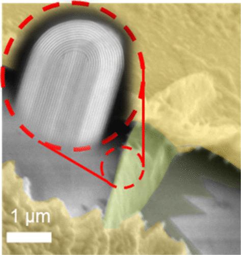
Transition metal dichalcogenides, notably MoS2, have garnered substantial attention owing to their excellent optical and electrical properties. While various methods have been employed to grow MoS2, resulting in nanostructures with diverse dimensionalities, controlling the lattice orientation and synthesizing aligned nanostructures beyond 2D remain a formidable challenge. In this study, we report the epitaxial growth of aligned MoS2 nanofin-nanoribbon hybrids, each consisting of a horizontal nanoribbon with a vertical lamellar structure (“fin”) in its center. Structural analysis reveals epitaxial relations that induce the growth into three isomorphic orientations following the 3-fold symmetry of the C-plane sapphire substrate. The nanofin-nanoribbon hybrid was integrated into a fin-channel photodetector with response times on the scale of tens of μs and high photocurrent. Furthermore, the nanofin-nanoribbon hybrids are incorporated into n-type “fin-FET” transistors, showing on–off ratios on the order of ∼103 at room temperature. The performance of these devices is discussed in terms of the efficient fabrication process, devoid of postgrowth steps, and the unique dimensionality of the device, which realizes a high optical path in the fin-shaped channel. This work demonstrates the integration of MoS2 into efficient fin-channel electronic and optoelectronic devices, laying the foundation for large-scale integration of TMDs into devices with nonstandard channel configurations.
外延混合维MoS2纳米鳍-纳米带杂化及其在电子和光电子器件中的集成
过渡金属二硫化物,特别是二硫化钼,由于其优异的光学和电学性质而引起了人们的广泛关注。虽然已经采用了各种方法来生长二硫化钼,从而产生了不同尺寸的纳米结构,但控制晶格取向并合成二维以外的排列纳米结构仍然是一个巨大的挑战。在这项研究中,我们报道了定向MoS2纳米鳍-纳米带杂化的外延生长,每个杂化由一个水平纳米带和一个垂直片层结构(“鳍”)组成。结构分析揭示了外延关系诱导生长成三个同构取向,遵循c面蓝宝石衬底的三重对称。将纳米鳍-纳米带杂化材料集成到鳍-通道光电探测器中,其响应时间可达数十μs,具有较高的光电流。此外,纳米翅片-纳米带杂化体被整合到n型“翅片-场效应晶体管”中,在室温下显示出约103的通断比。从高效的制造工艺、无后生步骤和独特的器件尺寸等方面讨论了这些器件的性能,这些器件在鳍形通道中实现了高光程。这项工作展示了MoS2集成到高效的鳍通道电子和光电子器件中,为将tmd大规模集成到非标准通道配置的器件中奠定了基础。
本文章由计算机程序翻译,如有差异,请以英文原文为准。
求助全文
约1分钟内获得全文
求助全文
来源期刊

ACS Applied Materials & Interfaces
工程技术-材料科学:综合
CiteScore
16.00
自引率
6.30%
发文量
4978
审稿时长
1.8 months
期刊介绍:
ACS Applied Materials & Interfaces is a leading interdisciplinary journal that brings together chemists, engineers, physicists, and biologists to explore the development and utilization of newly-discovered materials and interfacial processes for specific applications. Our journal has experienced remarkable growth since its establishment in 2009, both in terms of the number of articles published and the impact of the research showcased. We are proud to foster a truly global community, with the majority of published articles originating from outside the United States, reflecting the rapid growth of applied research worldwide.
 求助内容:
求助内容: 应助结果提醒方式:


