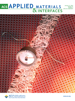
Constructing A Carrier Collection Framework at The Rear Interface in Cu2ZnSn(S, Se)4 Solar Cells by Selenizing an Inserted CuBi2O4 Nanolayer
IF 8.3
2区 材料科学
Q1 MATERIALS SCIENCE, MULTIDISCIPLINARY
引用次数: 0
Abstract
This work introduces the application of an ultrathin CuBi2O4 (CBO) nanolayer to improve the performance of Cu2ZnSn(S, Se)4 (CZTSSe) photovoltaic cells. The CBO layer is situated between molybdenum (Mo) and the CZTSSe absorber, which promotes the formation of a more compact absorber layer and larger CZTSSe grain sizes. Furthermore, the decomposition of the CBO layer during high-temperature annealing leads to the formation of Cu-doped bismuth selenide in the bottom region of the absorber. The Cu-doped bismuth selenide improves carrier transport and enhances the electrical properties at the rear interface of the CZTSSe device. These enhancements lead to notable improvements in all key photovoltaic parameters, thereby boosting the overall efficiency of the solar cell.

硒化CuBi2O4纳米层构建Cu2ZnSn(S, Se)4太阳能电池后界面载流子收集框架
本文介绍了超薄CuBi2O4 (CBO)纳米层在提高Cu2ZnSn(S, Se)4 (CZTSSe)光伏电池性能中的应用。CBO层位于钼(Mo)和CZTSSe吸收体之间,有利于形成致密的吸收层和较大的CZTSSe晶粒尺寸。此外,在高温退火过程中CBO层的分解导致吸收器底部区域形成cu掺杂的硒化铋。掺铜硒化铋改善了载流子输运,提高了器件后界面的电学性能。这些改进导致了所有关键光伏参数的显著改进,从而提高了太阳能电池的整体效率。
本文章由计算机程序翻译,如有差异,请以英文原文为准。
求助全文
约1分钟内获得全文
求助全文
来源期刊

ACS Applied Materials & Interfaces
工程技术-材料科学:综合
CiteScore
16.00
自引率
6.30%
发文量
4978
审稿时长
1.8 months
期刊介绍:
ACS Applied Materials & Interfaces is a leading interdisciplinary journal that brings together chemists, engineers, physicists, and biologists to explore the development and utilization of newly-discovered materials and interfacial processes for specific applications. Our journal has experienced remarkable growth since its establishment in 2009, both in terms of the number of articles published and the impact of the research showcased. We are proud to foster a truly global community, with the majority of published articles originating from outside the United States, reflecting the rapid growth of applied research worldwide.
 求助内容:
求助内容: 应助结果提醒方式:


