Vapour-deposited high-performance tin perovskite transistors
IF 40.9
1区 工程技术
Q1 ENGINEERING, ELECTRICAL & ELECTRONIC
引用次数: 0
Abstract
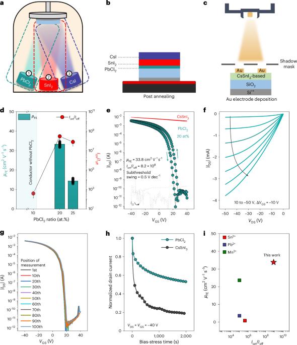
Solution-processed tin (Sn2+)-halide perovskites can be used to create p-channel thin-film transistors (TFTs) with performance levels comparable with commercial low-temperature polysilicon technology. However, high-quality perovskite film deposition using industry-compatible production techniques remains challenging. Here we report the fabrication of p-channel Sn2+-halide perovskite TFTs using a thermal evaporation approach with inorganic caesium tin iodide (CsSnI3). We use lead chloride (PbCl2) as a reaction initiator that triggers solid-state reactions of the as-evaporated perovskite compounds. This promotes the conversion of dense and uniform perovskite films, and also modulates the intrinsically high hole density of the CsSnI3 perovskite channels. Our optimized TFTs exhibit average hole field-effect mobilities of around 33.8 cm2 V−1 s−1, on/off current ratios of around 108, and large-area fabrication uniformity. The devices also exhibit improved stability compared with solution-deposited devices. Using a thermal evaporation approach and lead chloride (PbCl2) as a reaction initiator, caesium tin iodide (CsSnI3)-based p-channel thin-film transistors can be fabricated that exhibit average hole field-effect mobilities of around 33.8 cm2 V−1 s−1 and improved stability compared with solution-deposited devices.

气相沉积高性能锡钙钛矿晶体管
溶液处理锡(Sn2+)卤化物钙钛矿可用于制造p沟道薄膜晶体管(tft),其性能水平可与商业低温多晶硅技术相媲美。然而,使用工业兼容的生产技术进行高质量的钙钛矿薄膜沉积仍然具有挑战性。本文报道了用无机碘化锡铯(CsSnI3)热蒸发法制备p通道Sn2+卤化物钙钛矿tft。我们使用氯化铅(PbCl2)作为反应引发剂,触发作为蒸发的钙钛矿化合物的固态反应。这促进了致密均匀钙钛矿薄膜的转化,也调节了CsSnI3钙钛矿通道固有的高空穴密度。我们优化的TFTs平均空穴场效应迁移率约为33.8 cm2 V−1 s−1,开/关电流比约为108,大面积制造均匀性好。与溶液沉积器件相比,该器件还表现出更好的稳定性。
本文章由计算机程序翻译,如有差异,请以英文原文为准。
求助全文
约1分钟内获得全文
求助全文
来源期刊
Nature Electronics
Engineering-Electrical and Electronic Engineering
CiteScore
47.50
自引率
2.30%
发文量
159
期刊介绍:
Nature Electronics is a comprehensive journal that publishes both fundamental and applied research in the field of electronics. It encompasses a wide range of topics, including the study of new phenomena and devices, the design and construction of electronic circuits, and the practical applications of electronics. In addition, the journal explores the commercial and industrial aspects of electronics research.
The primary focus of Nature Electronics is on the development of technology and its potential impact on society. The journal incorporates the contributions of scientists, engineers, and industry professionals, offering a platform for their research findings. Moreover, Nature Electronics provides insightful commentary, thorough reviews, and analysis of the key issues that shape the field, as well as the technologies that are reshaping society.
Like all journals within the prestigious Nature brand, Nature Electronics upholds the highest standards of quality. It maintains a dedicated team of professional editors and follows a fair and rigorous peer-review process. The journal also ensures impeccable copy-editing and production, enabling swift publication. Additionally, Nature Electronics prides itself on its editorial independence, ensuring unbiased and impartial reporting.
In summary, Nature Electronics is a leading journal that publishes cutting-edge research in electronics. With its multidisciplinary approach and commitment to excellence, the journal serves as a valuable resource for scientists, engineers, and industry professionals seeking to stay at the forefront of advancements in the field.
 求助内容:
求助内容: 应助结果提醒方式:


