D. M. Kavya, Y. N. Sudhakar, A. Timoumi and Y. Raviprakash
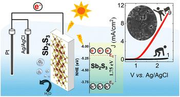
{"title":"Thickness-dependent performance of antimony sulfide thin films as a photoanode for enhanced photoelectrochemical water splitting","authors":"D. M. Kavya, Y. N. Sudhakar, A. Timoumi and Y. Raviprakash","doi":"10.1039/D5RA00586H","DOIUrl":null,"url":null,"abstract":"<p >A two-step synthesis approach is employed for antimony sulfide thin films, which includes thermal evaporation followed by annealing in a sulfur atmosphere using chemical vapor deposition (CVD). The thickness of the films is systematically varied to study its impact on the material's properties. The orthorhombic crystal structure of each film is verified by Grazing Incidence X-ray Diffraction (GIXRD) analysis. Raman spectroscopy reveals thickness-dependent changes in the vibrational properties. Surface morphology and roughness are examined using atomic force microscopy (AFM) and field emission scanning electron microscopy (FESEM), with findings indicating that layer thickness significantly affects these surface characteristics. Energy-dispersive X-ray spectroscopy (EDS) and X-ray photoelectron spectroscopy (XPS) demonstrate that variations in film thickness influence the surface chemical composition and oxidation states. The Sb<small><sub>2</sub></small>S<small><sub>3</sub></small> thin film with a thickness of 450 nm exhibited a band gap of 1.75 eV, indicating its potential for efficient light absorption. It also demonstrated a conductivity of 0.006 mA at an applied voltage of 1 V, reflecting its electrical transport properties. Furthermore, the film achieved a current density of 0.70 mA cm<small><sup>−2</sup></small>, signifying enhanced charge transfer efficiency. These findings suggest that the 450 nm thick film offers an optimal balance of band gap, light absorption, and photocurrent density, making it the most suitable candidate for photoelectrochemical water-splitting applications.</p>","PeriodicalId":102,"journal":{"name":"RSC Advances","volume":" 17","pages":" 13691-13702"},"PeriodicalIF":4.6000,"publicationDate":"2025-04-28","publicationTypes":"Journal Article","fieldsOfStudy":null,"isOpenAccess":false,"openAccessPdf":"https://pubs.rsc.org/en/content/articlepdf/2025/ra/d5ra00586h?page=search","citationCount":"0","resultStr":null,"platform":"Semanticscholar","paperid":null,"PeriodicalName":"RSC Advances","FirstCategoryId":"92","ListUrlMain":"https://pubs.rsc.org/en/content/articlelanding/2025/ra/d5ra00586h","RegionNum":3,"RegionCategory":"化学","ArticlePicture":[],"TitleCN":null,"AbstractTextCN":null,"PMCID":null,"EPubDate":"","PubModel":"","JCR":"Q2","JCRName":"CHEMISTRY, MULTIDISCIPLINARY","Score":null,"Total":0}
引用次数: 0
Abstract
A two-step synthesis approach is employed for antimony sulfide thin films, which includes thermal evaporation followed by annealing in a sulfur atmosphere using chemical vapor deposition (CVD). The thickness of the films is systematically varied to study its impact on the material's properties. The orthorhombic crystal structure of each film is verified by Grazing Incidence X-ray Diffraction (GIXRD) analysis. Raman spectroscopy reveals thickness-dependent changes in the vibrational properties. Surface morphology and roughness are examined using atomic force microscopy (AFM) and field emission scanning electron microscopy (FESEM), with findings indicating that layer thickness significantly affects these surface characteristics. Energy-dispersive X-ray spectroscopy (EDS) and X-ray photoelectron spectroscopy (XPS) demonstrate that variations in film thickness influence the surface chemical composition and oxidation states. The Sb2S3 thin film with a thickness of 450 nm exhibited a band gap of 1.75 eV, indicating its potential for efficient light absorption. It also demonstrated a conductivity of 0.006 mA at an applied voltage of 1 V, reflecting its electrical transport properties. Furthermore, the film achieved a current density of 0.70 mA cm−2, signifying enhanced charge transfer efficiency. These findings suggest that the 450 nm thick film offers an optimal balance of band gap, light absorption, and photocurrent density, making it the most suitable candidate for photoelectrochemical water-splitting applications.
期刊介绍:
An international, peer-reviewed journal covering all of the chemical sciences, including multidisciplinary and emerging areas. RSC Advances is a gold open access journal allowing researchers free access to research articles, and offering an affordable open access publishing option for authors around the world.
 求助内容:
求助内容: 应助结果提醒方式:


