Experimental Demonstration of Conjugate Structured Illumination Microscopy (c-SIM) for Sensing Deep Subwavelength Perturbations in Background Nanopatterns

IF 6.5 1区 物理与天体物理 Q1 MATERIALS SCIENCE, MULTIDISCIPLINARY
Jinsong Zhang, Renjie Zhou, Nicholas X. Fang, Weijie Deng, Jinlong Zhu, Shiyuan Liu
{"title":"Experimental Demonstration of Conjugate Structured Illumination Microscopy (c-SIM) for Sensing Deep Subwavelength Perturbations in Background Nanopatterns","authors":"Jinsong Zhang, Renjie Zhou, Nicholas X. Fang, Weijie Deng, Jinlong Zhu, Shiyuan Liu","doi":"10.1021/acsphotonics.5c00227","DOIUrl":null,"url":null,"abstract":"The localization and classification of deep-subwavelength objects embedded in dense background nanopatterns in an imaging mode are challenging because of the optical diffraction limit and the weak signal-to-noise ratio and contrast. In this work, we, for the first time, experimentally validated the proposed conjugate structured illumination microscopy (c-SIM), which utilizes optical proximity correction techniques to generate a wide-field, diffraction-limited, and structured illumination field on the sample surface for defect inspection. Our experiments validated that c-SIM could accurately inspect 29 nm wide defects with an enhanced resolution (half of the diffraction barrier) using a 423 nm laser source. Moreover, our investigation demonstrated that different types of 38 nm wide defects could be precisely pinpointed and directly classified from the captured frames in the lateral scanning process, which is attributed to the fact that a conjugate structured light field could induce a high-intensity gradient in the illumination light. This technology may find diverse applications, such as a patterned wafer defect inspection, photomask inspection, material characterization, metamaterial inspection, and nanosensing.","PeriodicalId":23,"journal":{"name":"ACS Photonics","volume":"2 1","pages":""},"PeriodicalIF":6.5000,"publicationDate":"2025-04-24","publicationTypes":"Journal Article","fieldsOfStudy":null,"isOpenAccess":false,"openAccessPdf":"","citationCount":"0","resultStr":null,"platform":"Semanticscholar","paperid":null,"PeriodicalName":"ACS Photonics","FirstCategoryId":"101","ListUrlMain":"https://doi.org/10.1021/acsphotonics.5c00227","RegionNum":1,"RegionCategory":"物理与天体物理","ArticlePicture":[],"TitleCN":null,"AbstractTextCN":null,"PMCID":null,"EPubDate":"","PubModel":"","JCR":"Q1","JCRName":"MATERIALS SCIENCE, MULTIDISCIPLINARY","Score":null,"Total":0}
引用次数: 0

Abstract

The localization and classification of deep-subwavelength objects embedded in dense background nanopatterns in an imaging mode are challenging because of the optical diffraction limit and the weak signal-to-noise ratio and contrast. In this work, we, for the first time, experimentally validated the proposed conjugate structured illumination microscopy (c-SIM), which utilizes optical proximity correction techniques to generate a wide-field, diffraction-limited, and structured illumination field on the sample surface for defect inspection. Our experiments validated that c-SIM could accurately inspect 29 nm wide defects with an enhanced resolution (half of the diffraction barrier) using a 423 nm laser source. Moreover, our investigation demonstrated that different types of 38 nm wide defects could be precisely pinpointed and directly classified from the captured frames in the lateral scanning process, which is attributed to the fact that a conjugate structured light field could induce a high-intensity gradient in the illumination light. This technology may find diverse applications, such as a patterned wafer defect inspection, photomask inspection, material characterization, metamaterial inspection, and nanosensing.

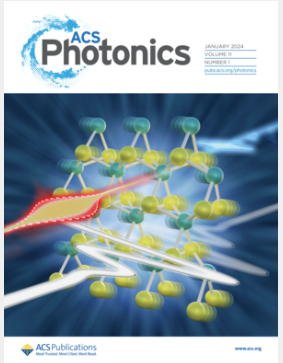
Abstract Image

共轭结构照明显微镜(c-SIM)用于检测背景纳米图案中深亚波长扰动的实验演示
由于光学衍射极限和较弱的信噪比和对比度,成像模式下深亚波长物体的定位和分类具有挑战性。在这项工作中,我们首次通过实验验证了所提出的共轭结构照明显微镜(c-SIM),该显微镜利用光学接近校正技术在样品表面产生宽视场,衍射受限的结构照明场,用于缺陷检测。实验证明,使用423 nm激光源,c-SIM可以精确检测29 nm宽的缺陷,并且分辨率提高(衍射势垒的一半)。此外,我们的研究表明,在横向扫描过程中,可以从捕获的帧中精确定位和直接分类不同类型的38 nm宽缺陷,这归因于共轭结构光场可以在照明光中诱导高强度梯度。这项技术可能会有不同的应用,如图像化晶圆缺陷检测、光掩膜检测、材料表征、超材料检测和纳米传感。
本文章由计算机程序翻译,如有差异,请以英文原文为准。
求助全文
约1分钟内获得全文 求助全文
来源期刊
ACS Photonics
ACS Photonics NANOSCIENCE & NANOTECHNOLOGY-MATERIALS SCIENCE, MULTIDISCIPLINARY
CiteScore
11.90
自引率
5.70%
发文量
438
审稿时长
2.3 months
期刊介绍: Published as soon as accepted and summarized in monthly issues, ACS Photonics will publish Research Articles, Letters, Perspectives, and Reviews, to encompass the full scope of published research in this field.
×
引用
GB/T 7714-2015
复制
MLA
复制
APA
复制
导出至
BibTeX EndNote RefMan NoteFirst NoteExpress
×
提示
您的信息不完整,为了账户安全,请先补充。
现在去补充
×
提示
您因"违规操作"
具体请查看互助需知
我知道了
×
提示
确定
请完成安全验证×
copy
已复制链接
快去分享给好友吧!
我知道了
右上角分享
点击右上角分享
0
联系我们:info@booksci.cn Book学术提供免费学术资源搜索服务,方便国内外学者检索中英文文献。致力于提供最便捷和优质的服务体验。 Copyright © 2023 布克学术 All rights reserved.
京ICP备2023020795号-1
ghs 京公网安备 11010802042870号
Book学术文献互助
Book学术文献互助群
群 号:481959085
Book学术官方微信