Quantum Dots Short-Wave Infrared Image Sensor with Enhanced Photoresponse Enabled by a Planar p–n Homojunction

IF 6.5 1区 物理与天体物理 Q1 MATERIALS SCIENCE, MULTIDISCIPLINARY
Yan Wang, Jieyu Zhang, Yingjie Tang, Yitong Chen, Dingwei Li, Huihui Ren, Fanfan Li, Guolei Liu, Qi Huang, Botao Ji, Bowen Zhu
{"title":"Quantum Dots Short-Wave Infrared Image Sensor with Enhanced Photoresponse Enabled by a Planar p–n Homojunction","authors":"Yan Wang, Jieyu Zhang, Yingjie Tang, Yitong Chen, Dingwei Li, Huihui Ren, Fanfan Li, Guolei Liu, Qi Huang, Botao Ji, Bowen Zhu","doi":"10.1021/acsphotonics.5c00231","DOIUrl":null,"url":null,"abstract":"Quantum dots (QDs)-based photodetectors are promising alternatives to construct short-wave infrared (SWIR) image sensors at a low cost. Improving the photoresponse and scalability of QDs is important to enable their practical applications. In this work, we developed a complementary metal–oxide–semiconductor (CMOS)-compatible SWIR image sensor based on lead sulfide (PbS) quantum dots (QDs) utilizing a p–n homojunction photoconductor (PC) architecture. Through solution-phase ligand-exchanged PbS QDs treated by lead iodide (PbI<sub>2</sub>) combined with a solid-state ligand-exchanged PbS QDs thin film treated with ethanedithiol (EDT), a p–n homojunction was constructed, enabling more efficient separation of photogenerated carriers and significantly enhancing the photoresponse. This approach allows for the monolithic integration of solution-processed QDs with silicon readout integrated circuits (ROICs), eliminating the need for complex flip-chip bonding and facilitating the fabrication of large-scale (640 × 512) QDs imagers. Consequently, the homojunction-based QDs SWIR imager delivers performance with low noise and a high average detectivity of 1.7 × 10<sup>10</sup> Jones, and the capability to capture high-resolution SWIR images highlights its potential for diverse applications.","PeriodicalId":23,"journal":{"name":"ACS Photonics","volume":"5 1","pages":""},"PeriodicalIF":6.5000,"publicationDate":"2025-04-23","publicationTypes":"Journal Article","fieldsOfStudy":null,"isOpenAccess":false,"openAccessPdf":"","citationCount":"0","resultStr":null,"platform":"Semanticscholar","paperid":null,"PeriodicalName":"ACS Photonics","FirstCategoryId":"101","ListUrlMain":"https://doi.org/10.1021/acsphotonics.5c00231","RegionNum":1,"RegionCategory":"物理与天体物理","ArticlePicture":[],"TitleCN":null,"AbstractTextCN":null,"PMCID":null,"EPubDate":"","PubModel":"","JCR":"Q1","JCRName":"MATERIALS SCIENCE, MULTIDISCIPLINARY","Score":null,"Total":0}
引用次数: 0

Abstract

Quantum dots (QDs)-based photodetectors are promising alternatives to construct short-wave infrared (SWIR) image sensors at a low cost. Improving the photoresponse and scalability of QDs is important to enable their practical applications. In this work, we developed a complementary metal–oxide–semiconductor (CMOS)-compatible SWIR image sensor based on lead sulfide (PbS) quantum dots (QDs) utilizing a p–n homojunction photoconductor (PC) architecture. Through solution-phase ligand-exchanged PbS QDs treated by lead iodide (PbI2) combined with a solid-state ligand-exchanged PbS QDs thin film treated with ethanedithiol (EDT), a p–n homojunction was constructed, enabling more efficient separation of photogenerated carriers and significantly enhancing the photoresponse. This approach allows for the monolithic integration of solution-processed QDs with silicon readout integrated circuits (ROICs), eliminating the need for complex flip-chip bonding and facilitating the fabrication of large-scale (640 × 512) QDs imagers. Consequently, the homojunction-based QDs SWIR imager delivers performance with low noise and a high average detectivity of 1.7 × 10¹⁰ Jones, and the capability to capture high-resolution SWIR images highlights its potential for diverse applications.

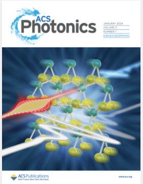
Abstract Image

平面p-n同质结增强光响应的量子点短波红外图像传感器
基于量子点(QDs)的光电探测器是低成本构建短波红外(SWIR)图像传感器的有希望的替代方案。提高量子点的光响应和可扩展性对其实际应用具有重要意义。在这项工作中,我们开发了一种互补金属氧化物半导体(CMOS)兼容的SWIR图像传感器,该传感器基于硫化铅(PbS)量子点(QDs),利用p-n同质结光导体(PC)架构。通过碘化铅(PbI2)处理的溶液相配体交换PbS量子点与乙二醇(EDT)处理的固态配体交换PbS量子点薄膜结合,构建了p-n同质结,使光生载流子更有效地分离,并显著增强了光响应。这种方法允许溶液处理的量子点与硅读出集成电路(roic)的单片集成,消除了复杂的倒装芯片键合的需要,并促进了大规模(640 × 512)量子点成像仪的制造。因此,基于同结的QDs SWIR成像仪具有低噪声和1.7 × 10¹⁰ Jones的高平均探测率的性能,并且能够捕获高分辨率SWIR图像,突出了其在各种应用中的潜力。
本文章由计算机程序翻译,如有差异,请以英文原文为准。
求助全文
约1分钟内获得全文 求助全文
来源期刊
ACS Photonics
ACS Photonics NANOSCIENCE & NANOTECHNOLOGY-MATERIALS SCIENCE, MULTIDISCIPLINARY
CiteScore
11.90
自引率
5.70%
发文量
438
审稿时长
2.3 months
期刊介绍: Published as soon as accepted and summarized in monthly issues, ACS Photonics will publish Research Articles, Letters, Perspectives, and Reviews, to encompass the full scope of published research in this field.
×
引用
GB/T 7714-2015
复制
MLA
复制
APA
复制
导出至
BibTeX EndNote RefMan NoteFirst NoteExpress
×
提示
您的信息不完整,为了账户安全,请先补充。
现在去补充
×
提示
您因"违规操作"
具体请查看互助需知
我知道了
×
提示
确定
请完成安全验证×
copy
已复制链接
快去分享给好友吧!
我知道了
右上角分享
点击右上角分享
0
联系我们:info@booksci.cn Book学术提供免费学术资源搜索服务,方便国内外学者检索中英文文献。致力于提供最便捷和优质的服务体验。 Copyright © 2023 布克学术 All rights reserved.
京ICP备2023020795号-1
ghs 京公网安备 11010802042870号
Book学术文献互助
Book学术文献互助群
群 号:481959085
Book学术官方微信