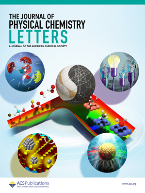
Single-Elemental Seamless Metal–Semiconductor Junctions Based on 2D Bi or Sb: Carrier Transport and Ultrafast Dynamics Study
IF 4.8
2区 化学
Q2 CHEMISTRY, PHYSICAL
引用次数: 0
Abstract
Two-dimensional (2D) metal–semiconductor (MS) junctions with their atomically thin nature are crucial for nanoelectronics. However, van der Waals (vdW) junctions face interfacial tunneling barriers, and lateral junctions suffer from chemical bonding disorders, both limiting carrier transport. Herein, based on the layer-dependent semiconductor-to-semimetal transition in 2D bismuthene (Bi) and antimonene (Sb), lateral seamless MS junctions with native chemical bonds are constructed to inhibit tunneling barriers and produce high-quality interfaces. These coherent junctions exhibit superior transport properties, yielding a significant current response at moderate bias as continuous covalent bonding removes vdW gaps and defects. In optoelectronic applications, the photogenerated carrier lifetimes in Bi and Sb reach 61.62 and 286.16 ns owing to weak electron–phonon coupling. Furthermore, the transport and optoelectronic properties of these MS junctions exhibit superior environmental resistance, while O2-induced trap states in Sb enhance photoconductive gain. This work provides a theoretical foundation for designing high-performance electronic and optoelectronic devices.

基于二维铋或锑的单元素无缝金属-半导体结:载流子输运和超快动力学研究
二维(2D)金属半导体(MS)结具有原子薄的性质,对纳米电子学至关重要。然而,范德华结(vdW)面临界面隧道障碍,横向结遭受化学键障碍,两者都限制了载流子的运输。本文基于二维铋烯(Bi)和锑烯(Sb)中依赖于层的半导体到半金属的转变,构建了具有天然化学键的横向无缝MS连接,以抑制隧道障碍并产生高质量的界面。这些相干结表现出优越的传输特性,在中等偏置下产生显著的电流响应,因为连续的共价键可以消除vdW的间隙和缺陷。在光电应用中,由于弱电子-声子耦合,Bi和Sb的光生载流子寿命分别达到61.62和286.16 ns。此外,这些MS结的输运和光电子特性表现出优异的环境抗性,而Sb中o2诱导的陷阱态增强了光导增益。该工作为设计高性能电子和光电子器件提供了理论基础。
本文章由计算机程序翻译,如有差异,请以英文原文为准。
求助全文
约1分钟内获得全文
求助全文
来源期刊

The Journal of Physical Chemistry Letters
CHEMISTRY, PHYSICAL-NANOSCIENCE & NANOTECHNOLOGY
CiteScore
9.60
自引率
7.00%
发文量
1519
审稿时长
1.6 months
期刊介绍:
The Journal of Physical Chemistry (JPC) Letters is devoted to reporting new and original experimental and theoretical basic research of interest to physical chemists, biophysical chemists, chemical physicists, physicists, material scientists, and engineers. An important criterion for acceptance is that the paper reports a significant scientific advance and/or physical insight such that rapid publication is essential. Two issues of JPC Letters are published each month.
 求助内容:
求助内容: 应助结果提醒方式:


