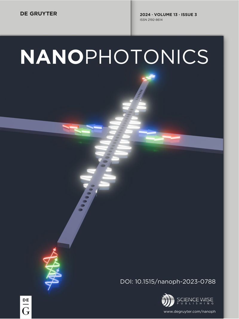
Inverse design of 3D nanophotonic devices with structural integrity using auxiliary thermal solvers
IF 6.5
2区 物理与天体物理
Q1 MATERIALS SCIENCE, MULTIDISCIPLINARY
引用次数: 0
Abstract
3D additive manufacturing enables the fabrication of nanophotonic structures with subwavelength features that control light across macroscopic scales. Gradient-based optimization offers an efficient approach to design these complex and non-intuitive structures. However, expanding this methodology from 2D to 3D introduces complexities, such as the need for structural integrity and connectivity. This work introduces a multi-objective optimization method to address these challenges in 3D nanophotonic designs. Our method combines electromagnetic simulations with an auxiliary heat-diffusion solver to ensure continuous material and void connectivity. By modeling material regions as heat sources and boundaries as heat sinks, we optimize the structure to minimize the total temperature, thereby penalizing disconnected regions that cannot dissipate thermal loads. Alongside the optical response, this heat metric becomes part of our objective function. We demonstrate the utility of our algorithm by designing two 3D nanophotonic devices. The first is a focusing element. The second is a waveguide junction, which connects two incoming waveguides for two different wavelengths into two outgoing waveguides, which are rotated by 90° to the incoming waveguides. Our approach offers a design pipeline that generates digital blueprints for fabricable nanophotonic materials, paving the way for practical 3D nanoprinting applications.基于辅助热求解器的结构完整三维纳米光子器件反设计
三维增材制造技术能够制造出具有亚波长特征的纳米光子结构,从而在宏观尺度上控制光线。基于梯度的优化为设计这些复杂而非直观的结构提供了一种有效的方法。然而,将这种方法从二维扩展到三维会带来一些复杂问题,如结构完整性和连通性的需要。这项工作引入了一种多目标优化方法,以应对三维纳米光子设计中的这些挑战。我们的方法将电磁模拟与辅助热扩散求解器相结合,以确保材料和空隙的连续连接。通过将材料区域建模为热源,将边界建模为散热器,我们优化了结构,使总温度降到最低,从而减少了无法消散热负荷的断开区域。除了光学响应之外,这一热量指标也成为我们目标函数的一部分。我们通过设计两个三维纳米光子器件来展示我们算法的实用性。第一个是聚焦元件。第二个是波导结,它将两个不同波长的入射波导连接到两个出射波导,出射波导与入射波导旋转 90°。我们的方法提供了一个设计管道,可生成可制造纳米光子材料的数字蓝图,为实际的三维纳米打印应用铺平了道路。
本文章由计算机程序翻译,如有差异,请以英文原文为准。
求助全文
约1分钟内获得全文
求助全文
来源期刊

Nanophotonics
NANOSCIENCE & NANOTECHNOLOGY-MATERIALS SCIENCE, MULTIDISCIPLINARY
CiteScore
13.50
自引率
6.70%
发文量
358
审稿时长
7 weeks
期刊介绍:
Nanophotonics, published in collaboration with Sciencewise, is a prestigious journal that showcases recent international research results, notable advancements in the field, and innovative applications. It is regarded as one of the leading publications in the realm of nanophotonics and encompasses a range of article types including research articles, selectively invited reviews, letters, and perspectives.
The journal specifically delves into the study of photon interaction with nano-structures, such as carbon nano-tubes, nano metal particles, nano crystals, semiconductor nano dots, photonic crystals, tissue, and DNA. It offers comprehensive coverage of the most up-to-date discoveries, making it an essential resource for physicists, engineers, and material scientists.
 求助内容:
求助内容: 应助结果提醒方式:


