CMOS-Compatible Fabrication of 2D Semiconductor-Based CFETs via High-k Dielectric van der Waals Encapsulation
IF 9.1
1区 材料科学
Q1 CHEMISTRY, MULTIDISCIPLINARY
引用次数: 0
Abstract
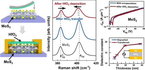
Two-dimensional (2D) semiconductors are potential candidates for advanced technology nodes, but their integration with silicon lines remains a significant challenge. Here, we present a high-k dielectric van der Waals encapsulation strategy for the fabrication of 2D semiconductor-based complementary field-effect transistors (CFETs) compatible with established processes. This technique, involving the transfer of a high-k dielectric onto 2D semiconductors, protects channels from polymer contamination, enables O2 plasma surface cleaning, and facilitates the following dielectric depositions without doping or damage. The strategy results in heterostructures and devices with reduced surface roughness and is applicable to both p- and n-type semiconductors, including MoS2, WS2, MoTe2, and black phosphorus. Utilizing this method, we have successfully fabricated 2D CFET inverters with a gain of up to 19.54 and power consumption as low as 2.63 nW. Our work paves the way for the integration of 2D semiconductors with silicon technology, therefore accelerating the lab-to-fab transition progress.
基于高k介电范德华封装的二维半导体cfet的cmos兼容制造
二维(2D)半导体是先进技术节点的潜在候选者,但它们与硅线的集成仍然是一个重大挑战。在这里,我们提出了一种高k介电范德瓦尔斯封装策略,用于制造与既定工艺兼容的二维半导体互补场效应晶体管(cfet)。该技术涉及将高k介电介质转移到2D半导体上,保护通道免受聚合物污染,使O2等离子体表面清洁,并促进后续介电沉积而不掺杂或损坏。该策略导致异质结构和器件表面粗糙度降低,适用于p型和n型半导体,包括MoS2, WS2, MoTe2和黑磷。利用这种方法,我们成功地制作了增益高达19.54,功耗低至2.63 nW的二维CFET逆变器。我们的工作为二维半导体与硅技术的集成铺平了道路,从而加速了从实验室到晶圆厂的过渡进程。
本文章由计算机程序翻译,如有差异,请以英文原文为准。
求助全文
约1分钟内获得全文
求助全文
来源期刊

Nano Letters
工程技术-材料科学:综合
CiteScore
16.80
自引率
2.80%
发文量
1182
审稿时长
1.4 months
期刊介绍:
Nano Letters serves as a dynamic platform for promptly disseminating original results in fundamental, applied, and emerging research across all facets of nanoscience and nanotechnology. A pivotal criterion for inclusion within Nano Letters is the convergence of at least two different areas or disciplines, ensuring a rich interdisciplinary scope. The journal is dedicated to fostering exploration in diverse areas, including:
- Experimental and theoretical findings on physical, chemical, and biological phenomena at the nanoscale
- Synthesis, characterization, and processing of organic, inorganic, polymer, and hybrid nanomaterials through physical, chemical, and biological methodologies
- Modeling and simulation of synthetic, assembly, and interaction processes
- Realization of integrated nanostructures and nano-engineered devices exhibiting advanced performance
- Applications of nanoscale materials in living and environmental systems
Nano Letters is committed to advancing and showcasing groundbreaking research that intersects various domains, fostering innovation and collaboration in the ever-evolving field of nanoscience and nanotechnology.
 求助内容:
求助内容: 应助结果提醒方式:


