Enhancing the Carrier Transport in Dielectric Passivation Layers via the Introduction of Trap States toward Improved CH3NH3PbI3/Si Heterojunction Photodetectors

IF 8.3 2区 材料科学 Q1 MATERIALS SCIENCE, MULTIDISCIPLINARY
Pengyu Chen, Jianxiang Huang, Guipeng Li, Hongping Li, Huimin Zhang, Chenglin Zhang, Yuan Liu, Dawei Cao, Mingming Chen
{"title":"Enhancing the Carrier Transport in Dielectric Passivation Layers via the Introduction of Trap States toward Improved CH3NH3PbI3/Si Heterojunction Photodetectors","authors":"Pengyu Chen, Jianxiang Huang, Guipeng Li, Hongping Li, Huimin Zhang, Chenglin Zhang, Yuan Liu, Dawei Cao, Mingming Chen","doi":"10.1021/acsami.5c03138","DOIUrl":null,"url":null,"abstract":"Dielectric thin layers have commonly been employed to passivate interfacial defects to improve the performance of heterojunction photodetectors (PDs), whereas their insulating nature severely hinders the out-of-plane carrier transport, thereby limiting the improvements in performance. Fortunately, such a problem can be well addressed by modulating the charge carriers’ transport process by introducing trap states. Herein, we reported the fabrication of much-improved CH<sub>3</sub>NH<sub>3</sub>PbI<sub>3</sub>/Si heterojunction PDs achieved by employing a HfO<sub>2+<i>x</i></sub> thin film with high-density (OH)<sub>O</sub> (i.e., OH substitute for O lattice site) as the interfacial passivation layer. Theoretical studies suggested that (OH)<sub>O</sub> defects have a low formation energy and exhibit hole-trapping behaviors. Notably, the interfacial passivation effects of the HfO<sub>2+<i>x</i></sub> thin films are comparable to those of the HfO<sub>2</sub> thin films. In addition, the out-of-plane hole transport was enhanced in the HfO<sub>2+<i>x</i></sub> thin films benefiting from the efficient (OH)<sub>O</sub> trap-assisted transport of holes. Finally, the performance of HfO<sub>2+<i>x</i></sub>-passivated PDs was remarkably improved. It is believed that the results demonstrated in this work provide a promising strategy for the fabrication of efficient heterojunction PDs in the future.","PeriodicalId":5,"journal":{"name":"ACS Applied Materials & Interfaces","volume":"25 1","pages":""},"PeriodicalIF":8.3000,"publicationDate":"2025-03-28","publicationTypes":"Journal Article","fieldsOfStudy":null,"isOpenAccess":false,"openAccessPdf":"","citationCount":"0","resultStr":null,"platform":"Semanticscholar","paperid":null,"PeriodicalName":"ACS Applied Materials & Interfaces","FirstCategoryId":"88","ListUrlMain":"https://doi.org/10.1021/acsami.5c03138","RegionNum":2,"RegionCategory":"材料科学","ArticlePicture":[],"TitleCN":null,"AbstractTextCN":null,"PMCID":null,"EPubDate":"","PubModel":"","JCR":"Q1","JCRName":"MATERIALS SCIENCE, MULTIDISCIPLINARY","Score":null,"Total":0}
引用次数: 0

Abstract

Dielectric thin layers have commonly been employed to passivate interfacial defects to improve the performance of heterojunction photodetectors (PDs), whereas their insulating nature severely hinders the out-of-plane carrier transport, thereby limiting the improvements in performance. Fortunately, such a problem can be well addressed by modulating the charge carriers’ transport process by introducing trap states. Herein, we reported the fabrication of much-improved CH3NH3PbI3/Si heterojunction PDs achieved by employing a HfO2+x thin film with high-density (OH)O (i.e., OH substitute for O lattice site) as the interfacial passivation layer. Theoretical studies suggested that (OH)O defects have a low formation energy and exhibit hole-trapping behaviors. Notably, the interfacial passivation effects of the HfO2+x thin films are comparable to those of the HfO2 thin films. In addition, the out-of-plane hole transport was enhanced in the HfO2+x thin films benefiting from the efficient (OH)O trap-assisted transport of holes. Finally, the performance of HfO2+x-passivated PDs was remarkably improved. It is believed that the results demonstrated in this work provide a promising strategy for the fabrication of efficient heterojunction PDs in the future.

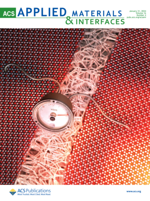
Abstract Image

求助全文
约1分钟内获得全文 求助全文
来源期刊
ACS Applied Materials & Interfaces
ACS Applied Materials & Interfaces 工程技术-材料科学:综合
CiteScore
16.00
自引率
6.30%
发文量
4978
审稿时长
1.8 months
期刊介绍: ACS Applied Materials & Interfaces is a leading interdisciplinary journal that brings together chemists, engineers, physicists, and biologists to explore the development and utilization of newly-discovered materials and interfacial processes for specific applications. Our journal has experienced remarkable growth since its establishment in 2009, both in terms of the number of articles published and the impact of the research showcased. We are proud to foster a truly global community, with the majority of published articles originating from outside the United States, reflecting the rapid growth of applied research worldwide.
×
引用
GB/T 7714-2015
复制
MLA
复制
APA
复制
导出至
BibTeX EndNote RefMan NoteFirst NoteExpress
×
提示
您的信息不完整,为了账户安全,请先补充。
现在去补充
×
提示
您因"违规操作"
具体请查看互助需知
我知道了
×
提示
确定
请完成安全验证×
copy
已复制链接
快去分享给好友吧!
我知道了
右上角分享
点击右上角分享
0
联系我们:info@booksci.cn Book学术提供免费学术资源搜索服务,方便国内外学者检索中英文文献。致力于提供最便捷和优质的服务体验。 Copyright © 2023 布克学术 All rights reserved.
京ICP备2023020795号-1
ghs 京公网安备 11010802042870号
Book学术文献互助
Book学术文献互助群
群 号:481959085
Book学术官方微信