Emerging Trends in Conductive Two-Dimensional Covalent Organic Frameworks for Large-Area Electronic Applications
IF 16
1区 材料科学
Q1 CHEMISTRY, MULTIDISCIPLINARY
引用次数: 0
Abstract
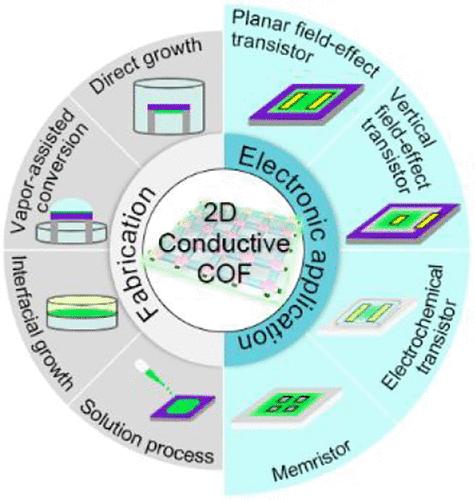
Two-dimensional covalent organic frameworks (2D COFs) are emerging as promising materials for advanced electronic applications due to their tunable porosity, crystalline order, and π-conjugated structures. These properties enable efficient charge transport and bandgap modulation, making 2D COFs strong candidates for electronic devices such as transistors and memristors. However, the practical application of COFs remains limited by challenges in achieving high-quality thin films with large-area uniformity and improved crystallinity. This review explores recent advancements in the fabrication and application of conductive 2D COFs for electronics. Various synthesis strategies, including direct growth, vapor-assisted conversion, and interfacial methods, are discussed in the context of enhancing film quality and scalability. The integration of COFs into electronic devices is classified based on their operation mechanism─planar and vertical field-effect transistors (FETs), electrochemical transistors (ECTs), and memristors─to highlight their electronic properties and device performance. Looking forward, the challenges of large-scale production, material compatibility, and device integration are outlined, alongside potential solutions through innovative synthesis techniques and collaborative research efforts. By addressing these challenges, 2D COFs are poised to drive breakthroughs in electronic devices by their adoption in next-generation semiconducting technologies.
用于大面积电子应用的导电二维共价有机框架的新趋势
二维共价有机框架(2D COFs)由于其可调的孔隙度、晶体有序度和π共轭结构而成为先进电子应用的有前途的材料。这些特性能够实现高效的电荷传输和带隙调制,使2D COFs成为晶体管和忆阻器等电子器件的有力候选材料。然而,COFs的实际应用仍然受到如何获得大面积均匀性和提高结晶度的高质量薄膜的挑战。本文综述了用于电子器件的导电二维COFs的制备和应用的最新进展。在提高薄膜质量和可扩展性的背景下,讨论了各种合成策略,包括直接生长,蒸汽辅助转化和界面方法。将COFs集成到电子器件中,根据其工作机制──平面场效应晶体管(fet)和垂直场效应晶体管(fet)、电化学晶体管(ECTs)和忆阻器──进行分类,以突出其电子特性和器件性能。展望未来,概述了大规模生产,材料兼容性和设备集成的挑战,以及通过创新合成技术和合作研究努力的潜在解决方案。通过解决这些挑战,2D COFs有望通过在下一代半导体技术中的应用来推动电子设备的突破。
本文章由计算机程序翻译,如有差异,请以英文原文为准。
求助全文
约1分钟内获得全文
求助全文
来源期刊

ACS Nano
工程技术-材料科学:综合
CiteScore
26.00
自引率
4.10%
发文量
1627
审稿时长
1.7 months
期刊介绍:
ACS Nano, published monthly, serves as an international forum for comprehensive articles on nanoscience and nanotechnology research at the intersections of chemistry, biology, materials science, physics, and engineering. The journal fosters communication among scientists in these communities, facilitating collaboration, new research opportunities, and advancements through discoveries. ACS Nano covers synthesis, assembly, characterization, theory, and simulation of nanostructures, nanobiotechnology, nanofabrication, methods and tools for nanoscience and nanotechnology, and self- and directed-assembly. Alongside original research articles, it offers thorough reviews, perspectives on cutting-edge research, and discussions envisioning the future of nanoscience and nanotechnology.
 求助内容:
求助内容: 应助结果提醒方式:


