Hyun Woo Tak, Chan Hyuk Choi, Seong Bae Kim, Myeong Ho Park, Jun Soo Lee, Akihide Sato, Bong Sun Kim, Jun Ki Jang, Eun Koo Kim, Dong Woo Kim* and Geun Young Yeom*,
{"title":"Effect of NF3, WF6, and MoF6 Additive Gases on High Aspect Ratio Contact SiO2 Etching in c-C4F8/C4F6/Ar/O2 Plasmas","authors":"Hyun Woo Tak, Chan Hyuk Choi, Seong Bae Kim, Myeong Ho Park, Jun Soo Lee, Akihide Sato, Bong Sun Kim, Jun Ki Jang, Eun Koo Kim, Dong Woo Kim* and Geun Young Yeom*, ","doi":"10.1021/acsaelm.4c0223910.1021/acsaelm.4c02239","DOIUrl":null,"url":null,"abstract":"<p >Etch profile control of high aspect ratio contact (HARC) is one of the key issues in developing next-generation memory device manufacturing because the HARC etch result can determine the device integration and device performance. In this study, the effect of F-based additive gases such as nitrogen trifluoride (NF<sub>3</sub>), tungsten hexafluoride (WF<sub>6</sub>), and molybdenum hexafluoride (MoF<sub>6</sub>) on the HARC SiO<sub>2</sub> etching was investigated. A few sccm of NF<sub>3</sub>, WF<sub>6</sub>, and MoF<sub>6</sub> added to the base gas recipe did not change the SiO<sub>2</sub> etch rate and etch selectivity over the amorphous carbon layer (ACL) noticeably. However, the addition of NF<sub>3</sub> flow enlarged the etched HARC SiO<sub>2</sub> top hole size by decreasing the polymer layer thickness deposited on the sidewall. On the contrary, metal-containing additive gases such as WF<sub>6</sub> and MoF<sub>6</sub> resulted in decreased HARC SiO<sub>2</sub> top hole size enlargement. For the base recipe and with NF<sub>3</sub> addition, distorted and oval-shaped SiO<sub>2</sub> bottom holes were observed possibly due to the charging of the SiO<sub>2</sub> sidewall during the etching. But, for the addition of WF<sub>6</sub> and MoF<sub>6</sub>, rather circular-shaped SiO<sub>2</sub> bottom holes could be observed possibly due to the decreased SiO<sub>2</sub> sidewall charging by the formation of a more conductive polymer through the inclusion of metals.</p>","PeriodicalId":3,"journal":{"name":"ACS Applied Electronic Materials","volume":"7 5","pages":"1953–1965 1953–1965"},"PeriodicalIF":4.7000,"publicationDate":"2025-02-19","publicationTypes":"Journal Article","fieldsOfStudy":null,"isOpenAccess":false,"openAccessPdf":"","citationCount":"0","resultStr":null,"platform":"Semanticscholar","paperid":null,"PeriodicalName":"ACS Applied Electronic Materials","FirstCategoryId":"88","ListUrlMain":"https://pubs.acs.org/doi/10.1021/acsaelm.4c02239","RegionNum":3,"RegionCategory":"材料科学","ArticlePicture":[],"TitleCN":null,"AbstractTextCN":null,"PMCID":null,"EPubDate":"","PubModel":"","JCR":"Q1","JCRName":"ENGINEERING, ELECTRICAL & ELECTRONIC","Score":null,"Total":0}
引用次数: 0
Abstract
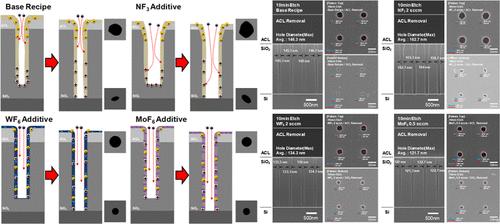
Etch profile control of high aspect ratio contact (HARC) is one of the key issues in developing next-generation memory device manufacturing because the HARC etch result can determine the device integration and device performance. In this study, the effect of F-based additive gases such as nitrogen trifluoride (NF3), tungsten hexafluoride (WF6), and molybdenum hexafluoride (MoF6) on the HARC SiO2 etching was investigated. A few sccm of NF3, WF6, and MoF6 added to the base gas recipe did not change the SiO2 etch rate and etch selectivity over the amorphous carbon layer (ACL) noticeably. However, the addition of NF3 flow enlarged the etched HARC SiO2 top hole size by decreasing the polymer layer thickness deposited on the sidewall. On the contrary, metal-containing additive gases such as WF6 and MoF6 resulted in decreased HARC SiO2 top hole size enlargement. For the base recipe and with NF3 addition, distorted and oval-shaped SiO2 bottom holes were observed possibly due to the charging of the SiO2 sidewall during the etching. But, for the addition of WF6 and MoF6, rather circular-shaped SiO2 bottom holes could be observed possibly due to the decreased SiO2 sidewall charging by the formation of a more conductive polymer through the inclusion of metals.
期刊介绍:
ACS Applied Electronic Materials is an interdisciplinary journal publishing original research covering all aspects of electronic materials. The journal is devoted to reports of new and original experimental and theoretical research of an applied nature that integrate knowledge in the areas of materials science, engineering, optics, physics, and chemistry into important applications of electronic materials. Sample research topics that span the journal's scope are inorganic, organic, ionic and polymeric materials with properties that include conducting, semiconducting, superconducting, insulating, dielectric, magnetic, optoelectronic, piezoelectric, ferroelectric and thermoelectric.
Indexed/Abstracted:
Web of Science SCIE
Scopus
CAS
INSPEC
Portico

 求助内容:
求助内容: 应助结果提醒方式:


