Reliability of the Transmission Line Method and Reproducibility of the Measured Contact Resistance of Organic Thin-Film Transistors

IF 15.8 1区 材料科学 Q1 CHEMISTRY, MULTIDISCIPLINARY
ACS Nano Pub Date : 2025-03-10 DOI:10.1021/acsnano.4c15828
Tobias Wollandt, Sabrina Steffens, Yurii Radiev, Florian Letzkus, Joachim N. Burghartz, Gregor Witte, Hagen Klauk
{"title":"Reliability of the Transmission Line Method and Reproducibility of the Measured Contact Resistance of Organic Thin-Film Transistors","authors":"Tobias Wollandt, Sabrina Steffens, Yurii Radiev, Florian Letzkus, Joachim N. Burghartz, Gregor Witte, Hagen Klauk","doi":"10.1021/acsnano.4c15828","DOIUrl":null,"url":null,"abstract":"Using the transmission line method (TLM), we extracted the contact resistance of organic thin-film transistors (TFTs) based on five different vacuum-deposited small-molecule semiconductors fabricated on over 500 substrates. In the first part of this report, we illustrate how the reliability of the TLM analysis is affected by the statistical uncertainty that arises from the fitting procedure and by the systematic error that is introduced if the actual channel length of the TFTs deviates from the nominal channel length. In the second part, we show that the contact resistance of organic TFTs varies significantly from one fabrication run to the next (and even across substrates fabricated within the same fabrication run), no matter how much care is taken to keep all controllable fabrication-process parameters constant. A statistical analysis reveals no strong correlations between the contact resistance and environmental parameters present during TFT fabrication, such as the humidity in the laboratory or the base pressure of the vacuum during material depositions. This suggests that the observed variation in the contact resistance is mainly stochastic. For the TFTs based on the best-performing semiconductor, the contact resistance varies between 28 Ωcm and 1 kΩcm, with a median value of 160 Ωcm.","PeriodicalId":21,"journal":{"name":"ACS Nano","volume":"53 1","pages":""},"PeriodicalIF":15.8000,"publicationDate":"2025-03-10","publicationTypes":"Journal Article","fieldsOfStudy":null,"isOpenAccess":false,"openAccessPdf":"","citationCount":"0","resultStr":null,"platform":"Semanticscholar","paperid":null,"PeriodicalName":"ACS Nano","FirstCategoryId":"88","ListUrlMain":"https://doi.org/10.1021/acsnano.4c15828","RegionNum":1,"RegionCategory":"材料科学","ArticlePicture":[],"TitleCN":null,"AbstractTextCN":null,"PMCID":null,"EPubDate":"","PubModel":"","JCR":"Q1","JCRName":"CHEMISTRY, MULTIDISCIPLINARY","Score":null,"Total":0}
引用次数: 0

Abstract

Using the transmission line method (TLM), we extracted the contact resistance of organic thin-film transistors (TFTs) based on five different vacuum-deposited small-molecule semiconductors fabricated on over 500 substrates. In the first part of this report, we illustrate how the reliability of the TLM analysis is affected by the statistical uncertainty that arises from the fitting procedure and by the systematic error that is introduced if the actual channel length of the TFTs deviates from the nominal channel length. In the second part, we show that the contact resistance of organic TFTs varies significantly from one fabrication run to the next (and even across substrates fabricated within the same fabrication run), no matter how much care is taken to keep all controllable fabrication-process parameters constant. A statistical analysis reveals no strong correlations between the contact resistance and environmental parameters present during TFT fabrication, such as the humidity in the laboratory or the base pressure of the vacuum during material depositions. This suggests that the observed variation in the contact resistance is mainly stochastic. For the TFTs based on the best-performing semiconductor, the contact resistance varies between 28 Ωcm and 1 kΩcm, with a median value of 160 Ωcm.

Abstract Image

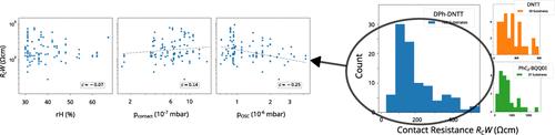
我们使用传输线法 (TLM) 提取了有机薄膜晶体管 (TFT) 的接触电阻,这些晶体管基于在 500 多种基板上制造的五种不同的真空沉积小分子半导体。在本报告的第一部分,我们说明了 TLM 分析的可靠性如何受到拟合过程中产生的统计不确定性以及 TFT 实际沟道长度偏离标称沟道长度时引入的系统误差的影响。在第二部分,我们展示了有机 TFT 的接触电阻在不同的制造流程(甚至在同一制造流程中制造的不同基板)之间存在显著差异,无论如何注意保持所有可控制造流程参数不变。统计分析表明,接触电阻与 TFT 制造过程中的环境参数(如实验室湿度或材料沉积过程中的真空基本压力)之间没有很强的相关性。这表明观察到的接触电阻变化主要是随机的。对于基于性能最佳半导体的 TFT,接触电阻在 28 Ωcm 和 1 kΩcm 之间变化,中值为 160 Ωcm。
本文章由计算机程序翻译,如有差异,请以英文原文为准。
求助全文
约1分钟内获得全文 求助全文
来源期刊
ACS Nano
ACS Nano 工程技术-材料科学:综合
CiteScore
26.00
自引率
4.10%
发文量
1627
审稿时长
1.7 months
期刊介绍: ACS Nano, published monthly, serves as an international forum for comprehensive articles on nanoscience and nanotechnology research at the intersections of chemistry, biology, materials science, physics, and engineering. The journal fosters communication among scientists in these communities, facilitating collaboration, new research opportunities, and advancements through discoveries. ACS Nano covers synthesis, assembly, characterization, theory, and simulation of nanostructures, nanobiotechnology, nanofabrication, methods and tools for nanoscience and nanotechnology, and self- and directed-assembly. Alongside original research articles, it offers thorough reviews, perspectives on cutting-edge research, and discussions envisioning the future of nanoscience and nanotechnology.
×
引用
GB/T 7714-2015
复制
MLA
复制
APA
复制
导出至
BibTeX EndNote RefMan NoteFirst NoteExpress
×
提示
您的信息不完整,为了账户安全,请先补充。
现在去补充
×
提示
您因"违规操作"
具体请查看互助需知
我知道了
×
提示
确定
请完成安全验证×
copy
已复制链接
快去分享给好友吧!
我知道了
右上角分享
点击右上角分享
0
联系我们:info@booksci.cn Book学术提供免费学术资源搜索服务,方便国内外学者检索中英文文献。致力于提供最便捷和优质的服务体验。 Copyright © 2023 布克学术 All rights reserved.
京ICP备2023020795号-1
ghs 京公网安备 11010802042870号
Book学术文献互助
Book学术文献互助群
群 号:481959085
Book学术官方微信