Synthetic Band Structure Engineering of Graphene Using Block Copolymer-Templated Dielectric Superlattices
IF 15.8
1区 材料科学
Q1 CHEMISTRY, MULTIDISCIPLINARY
引用次数: 0
Abstract
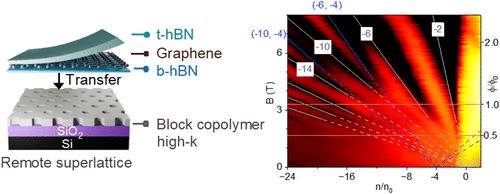
Engineering the electronic band structure of two-dimensional (2D) materials by imposing spatially periodic superlattice (SL) potentials opens a pathway to unconventional electronics. Nanopatterning the gate electrode or surface dielectric near 2D crystals provides a powerful strategy for realizing electrostatically tunable “remote” SLs with flexibility in lattice design. Here, we demonstrate the effectiveness of block copolymer (BCP)-templated dielectric nanopatterns for fabricating etch-free high-grade metal oxide SLs. Alumina (AlOx) nanopatterns with hexagonal symmetry and a 38 nm SL wavelength are produced as a model material by directly converting a self-assembled BCP film via block-selective vapor phase infiltration. Despite micrometer-scale rotational disorder inherent to BCP self-assembly, electronic transport measurements of graphene reveal replica Dirac points at zero field and Hofstadter mini-gaps under finite magnetic fields. These results indicate the successful formation of remote SL potentials in graphene resulting from optimized AlOx nanopattern fabrication to achieve consistent lattice symmetry and periodicity at a macroscopic scale. The findings of this study, combined with the versatile, scalable, and cost-effective nature of BCP nanopatterning, highlight the potential of BCP-templated nanostructures for remote SL engineering in 2D crystals.
求助全文
约1分钟内获得全文
求助全文
来源期刊

ACS Nano
工程技术-材料科学:综合
CiteScore
26.00
自引率
4.10%
发文量
1627
审稿时长
1.7 months
期刊介绍:
ACS Nano, published monthly, serves as an international forum for comprehensive articles on nanoscience and nanotechnology research at the intersections of chemistry, biology, materials science, physics, and engineering. The journal fosters communication among scientists in these communities, facilitating collaboration, new research opportunities, and advancements through discoveries. ACS Nano covers synthesis, assembly, characterization, theory, and simulation of nanostructures, nanobiotechnology, nanofabrication, methods and tools for nanoscience and nanotechnology, and self- and directed-assembly. Alongside original research articles, it offers thorough reviews, perspectives on cutting-edge research, and discussions envisioning the future of nanoscience and nanotechnology.
 求助内容:
求助内容: 应助结果提醒方式:


