Two-dimensional Bi2SeO2 and Its Native Insulators for Next-Generation Nanoelectronics
IF 15.8
1区 材料科学
Q1 CHEMISTRY, MULTIDISCIPLINARY
引用次数: 0
Abstract
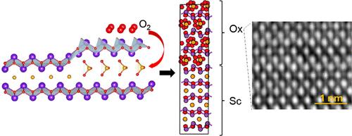
Silicon’s dominance in integrated circuits is largely due to its stable native oxide, SiO2, known for its insulating properties and excellent interface to the Si channel. However, silicon-based FETs face significant challenges when further scaled, which inspires the search for better semiconductors. While 2D materials such as MoS2, WSe2, BP, and InSe are promising, they lack a stable and compatible native oxide. High mobility (812 cm2 V–1 s–1) 2D Bi2SeO2 stands out in this regard, as it can be oxidized into different forms of Bi2SeO5, thereby forming compatible high-κ native oxides. Despite growing interest in this material system, a comprehensive understanding of its fundamental properties is lacking. This study uses density functional theory and molecular dynamics simulations to investigate the intrinsic properties of Bi2SeO2, its native oxides, and its interfaces. Additionally, scanning transmission electron microscopy is employed to complement these theoretical analyses, providing detailed insights into the atomic-scale structure and interfaces of these materials. Building on these findings, we model semiconductor-oxide heterostructures and extract their intrinsic properties. Our results demonstrate that the atomically sharp and clean interface between oxide and semiconductor, the high dielectric constant (>30) of the oxide, and the sufficiently large conduction band offsets between the semiconductor and the most relevant β-phase of its native insulator (1.13 eV for holes and 1.55 eV for electrons) make this material system a strong candidate for future transistor technologies. These properties mitigate the limitations of traditional semiconductors and enhance device performance at the ultimate scaling limit, positioning 2D Bi2SeO2 as a suitable choice for next-generation nanoelectronics.
求助全文
约1分钟内获得全文
求助全文
来源期刊

ACS Nano
工程技术-材料科学:综合
CiteScore
26.00
自引率
4.10%
发文量
1627
审稿时长
1.7 months
期刊介绍:
ACS Nano, published monthly, serves as an international forum for comprehensive articles on nanoscience and nanotechnology research at the intersections of chemistry, biology, materials science, physics, and engineering. The journal fosters communication among scientists in these communities, facilitating collaboration, new research opportunities, and advancements through discoveries. ACS Nano covers synthesis, assembly, characterization, theory, and simulation of nanostructures, nanobiotechnology, nanofabrication, methods and tools for nanoscience and nanotechnology, and self- and directed-assembly. Alongside original research articles, it offers thorough reviews, perspectives on cutting-edge research, and discussions envisioning the future of nanoscience and nanotechnology.
 求助内容:
求助内容: 应助结果提醒方式:


