Surface dipole induced Ohmic contact in two-dimensional Sc2CTT’/graphene heterostructures
IF 6.3
2区 材料科学
Q2 CHEMISTRY, PHYSICAL
引用次数: 0
Abstract
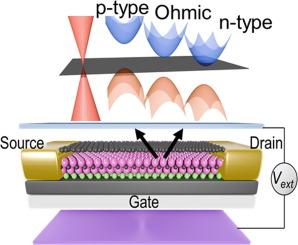
Schottky electrical contact occurs at the metal–semiconductor heterstructures (MSHs) that are comprised of metallic graphene eletrode and most of two-dimensional (2D) semiconductors, which seriously degrades the electronic devices’ performance. Herein, we proposed a family of 2D Sc2CTT’ semiconductors through eliminating the surface electrons of Sc2C electride. We exploited these Sc2CTT’ as channel materials to construct graphene-based MSHs and achieved their Ohmic contacts with low contact resistance. The Sc2CClH/graphene form a p-type Schottky contact (Shc) with a tiny SBH (∼0.1 eV), the Sc2CHCl/graphene exhibits a p-type Ohmic contact (Ohc), and the Sc2CClOH/graphene favors an intrinsic n-type Ohc. These excellent electric contacts are owing to the intrinsic and distinctive electronic characters where the band edge electronic states reside in the inner Sc2C layer while the outer H (or OH) and Cl layers only act as encapsulation layers. Furthermore, the p-type Shc easily transforms into the p-type Ohc for Sc2CClH/graphene, and the Ohc of Sc2CHCl/graphene and Sc2CClOH/graphene are well retained under perpendicular electric fields. This can be explained by the counteraction between external electric fields and intrinsic built-in electric fields. This study demonstrates that the surface dipole of 2D semiconductors with asymmetric bonding can greatly impact the interface contact properties.

求助全文
约1分钟内获得全文
求助全文
来源期刊

Applied Surface Science
工程技术-材料科学:膜
CiteScore
12.50
自引率
7.50%
发文量
3393
审稿时长
67 days
期刊介绍:
Applied Surface Science covers topics contributing to a better understanding of surfaces, interfaces, nanostructures and their applications. The journal is concerned with scientific research on the atomic and molecular level of material properties determined with specific surface analytical techniques and/or computational methods, as well as the processing of such structures.
 求助内容:
求助内容: 应助结果提醒方式:


