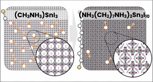
(NH3(CH2)7NH3)2Sn3I10, a Vacancy-Ordered Three-Dimensional Tin(II) Perovskite-Derived Semiconductor
IF 7.2
2区 材料科学
Q2 CHEMISTRY, PHYSICAL
引用次数: 0
Abstract
Ordering vacancies in hybrid Sn(II) halide semiconductors provides a strategy for preventing uncontrolled oxidation and formation of mobile holes. In this study, we report the structure and optical and electronic properties of (NH3(CH2)7NH3)2Sn3I10, a vacancy-ordered perovskite derivative with three-dimensional inorganic connectivity. The crystal structure resembles that of a Dion–Jacobson layered perovskite derivative, but with [SnI5] square pyramids bridging the layers. UV–vis diffuse reflectance spectroscopy reveals a sharp onset of light absorption at 1.86(1) eV with the photoluminescence emission maximum at 1.90(1) eV. However, the maximum excitation occurs from 3.42 to 3.81 eV (325 to 370 nm), revealing a significant Stokes shift of 1.3 eV. The electronic properties determined from dark and time-resolved microwave conductivity measurements reveal a minimum carrier mobility of 4.3 × 10⁻² cm2 V–1 s–1 and a maximum carrier density of 5.96 × 1016 cm–3, a uniquely low value for a hybrid Sn(II) halide semiconductor. The transport behavior in combination with first-principles calculations of the electronic band structure and dielectric permittivity suggest polaron-mediated electronic transport, yet the photogenerated carriers have a fast and fluence-dependent nonradiative recombination rate, suggestive of localized “defect-like” states at the band edge. The observed photoluminescence is most consistent with single-ion-like behavior of an asymmetric Sn(II) environment. Together, these results suggest that defect ordering presents a strategy for the reduction of mobile charge carriers at equilibrium.
求助全文
约1分钟内获得全文
求助全文
来源期刊
Chemistry of Materials
工程技术-材料科学:综合
CiteScore
14.10
自引率
5.80%
发文量
929
审稿时长
1.5 months
期刊介绍:
The journal Chemistry of Materials focuses on publishing original research at the intersection of materials science and chemistry. The studies published in the journal involve chemistry as a prominent component and explore topics such as the design, synthesis, characterization, processing, understanding, and application of functional or potentially functional materials. The journal covers various areas of interest, including inorganic and organic solid-state chemistry, nanomaterials, biomaterials, thin films and polymers, and composite/hybrid materials. The journal particularly seeks papers that highlight the creation or development of innovative materials with novel optical, electrical, magnetic, catalytic, or mechanical properties. It is essential that manuscripts on these topics have a primary focus on the chemistry of materials and represent a significant advancement compared to prior research. Before external reviews are sought, submitted manuscripts undergo a review process by a minimum of two editors to ensure their appropriateness for the journal and the presence of sufficient evidence of a significant advance that will be of broad interest to the materials chemistry community.
 求助内容:
求助内容: 应助结果提醒方式:


