Low-power 2D gate-all-around logics via epitaxial monolithic 3D integration
IF 37.2
1区 材料科学
Q1 CHEMISTRY, PHYSICAL
引用次数: 0
Abstract
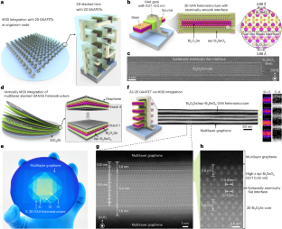
Innovations in device architectures and materials promote transistor miniaturization for improved performance, energy efficiency and integration density. At foreseeable ångström nodes, a gate-all-around (GAA) field-effect transistor based on two-dimensional (2D) semiconductors would provide excellent electrostatic gate controllability to achieve ultimate power scaling and performance delivering. However, a major roadblock lies in the scalable integration of 2D GAA heterostructures with atomically smooth and conformal interfaces. Here we report a wafer-scale multi-layer-stacked single-crystalline 2D GAA configuration achieved with low-temperature monolithic three-dimensional integration, in which high-mobility 2D semiconductor Bi2O2Se was epitaxially integrated by high-κ layered native-oxide dielectric Bi2SeO5 with an atomically smooth interface, enabling a high electron mobility of 280 cm2 V−1 s−1 and a near-ideal subthreshold swing of 62 mV dec−1. The scaled 2D GAA field-effect transistor with 30 nm gate length exhibits an ultralow operation voltage of 0.5 V, a high on-state current exceeding 1 mA μm−1, an ultralow intrinsic delay of 1.9 ps and an energy-delay product of 1.84 × 10⁻²⁷ Js μm−1. This work demonstrates a wafer-scale 2D-material-based GAA system with valid performance and power merits, holding promising prospects for beyond-silicon monolithic three-dimensional circuits. A multi-layer wafer-scale 2D gate-all-around system with an atomically smooth interface fabricated via epitaxial monolithic 3D integration shows good performance and power efficiency, holding promise for the forthcoming ångström technology node.

通过外延单片3D集成的低功耗2D栅极全能逻辑
器件架构和材料的创新促进了晶体管小型化,以提高性能、能源效率和集成密度。在可预见的ångström节点上,基于二维(2D)半导体的栅极全能(GAA)场效应晶体管将提供出色的静电栅极可控性,从而实现最终的功率缩放和性能交付。然而,一个主要的障碍在于具有原子光滑和保形界面的二维GAA异质结构的可扩展集成。本文报道了一种采用低温单片三维集成技术实现的晶圆级多层堆叠二维GAA结构,其中高迁移率的二维半导体Bi2O2Se被具有原子光滑界面的高κ层状天然氧化物介电Bi2SeO5外延集成,实现了280 cm2 V−1 s−1的高电子迁移率和接近理想的62 mV dec−1亚阈值摆幅。该栅极长度为30 nm的二维GAA场效应晶体管的超低工作电压为0.5 V,高导通电流超过1 mA μm−1,超低本构延迟为1.9 ps,能量延迟积为1.84 × 10⁻²⁷ Js μm−1。这项工作展示了一种基于晶圆级二维材料的GAA系统,具有有效的性能和功率优点,在超硅单片三维电路中具有良好的前景。
本文章由计算机程序翻译,如有差异,请以英文原文为准。
求助全文
约1分钟内获得全文
求助全文
来源期刊
Nature Materials
工程技术-材料科学:综合
CiteScore
62.20
自引率
0.70%
发文量
221
审稿时长
3.2 months
期刊介绍:
Nature Materials is a monthly multi-disciplinary journal aimed at bringing together cutting-edge research across the entire spectrum of materials science and engineering. It covers all applied and fundamental aspects of the synthesis/processing, structure/composition, properties, and performance of materials. The journal recognizes that materials research has an increasing impact on classical disciplines such as physics, chemistry, and biology.
Additionally, Nature Materials provides a forum for the development of a common identity among materials scientists and encourages interdisciplinary collaboration. It takes an integrated and balanced approach to all areas of materials research, fostering the exchange of ideas between scientists involved in different disciplines.
Nature Materials is an invaluable resource for scientists in academia and industry who are active in discovering and developing materials and materials-related concepts. It offers engaging and informative papers of exceptional significance and quality, with the aim of influencing the development of society in the future.
 求助内容:
求助内容: 应助结果提醒方式:


