Simultaneous Improvement of Multiple Electrical Characteristics in Ultrathin a-IGZO TFTs Using Machine Learning Optimization
IF 8.3
2区 材料科学
Q1 MATERIALS SCIENCE, MULTIDISCIPLINARY
引用次数: 0
Abstract
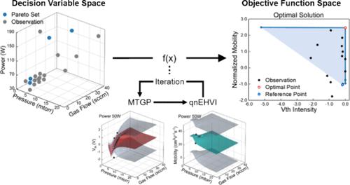
While IGZO is emerging as a promising channel material to address the scaling limitations of conventional silicon-based DRAM, its application in next-generation 3D DRAM requires further advancements in achieving ultrathin structures and excellent performance tailored to DRAM characteristics. Specifically, optimizing process variables is essential for enhancing mobility in ultrathin structures, where mobility tends to degrade significantly, while maintaining a constant threshold voltage, a task that is both experimentally intensive and resource-demanding. This study employed multi-objective Bayesian optimization (MOBO) machine learning (ML) to simultaneously optimize multiple electrical objectives, aiming to achieve high mobility and a near-zero threshold voltage for ultrathin IGZO thin-film transistors (TFTs) under complex sputtering conditions, involving a wide range of possible combinations of Ar gas flow, sputtering power, and working pressure. Integrating empirical insights and expert knowledge into feature extraction, the MOBO approach leveraged human-driven expertise to optimize field-effect mobility and threshold voltage within the solution space. With ML assistance, a Pareto-optimal front was constructed to visualize trade-offs, achieving high field-effect mobility of 33.1 cm2/V·s and near-zero threshold voltage of −0.05 V at a 7.47 nm channel thickness. This approach is expected advance next-generation semiconductor technologies, offering exceptional gains in both efficiency and performance.
求助全文
约1分钟内获得全文
求助全文
来源期刊

ACS Applied Materials & Interfaces
工程技术-材料科学:综合
CiteScore
16.00
自引率
6.30%
发文量
4978
审稿时长
1.8 months
期刊介绍:
ACS Applied Materials & Interfaces is a leading interdisciplinary journal that brings together chemists, engineers, physicists, and biologists to explore the development and utilization of newly-discovered materials and interfacial processes for specific applications. Our journal has experienced remarkable growth since its establishment in 2009, both in terms of the number of articles published and the impact of the research showcased. We are proud to foster a truly global community, with the majority of published articles originating from outside the United States, reflecting the rapid growth of applied research worldwide.
 求助内容:
求助内容: 应助结果提醒方式:


