Unveiling the Correlation between Defects and High Mobility in MoS2 Monolayers
IF 8.2
2区 材料科学
Q1 MATERIALS SCIENCE, MULTIDISCIPLINARY
引用次数: 0
Abstract
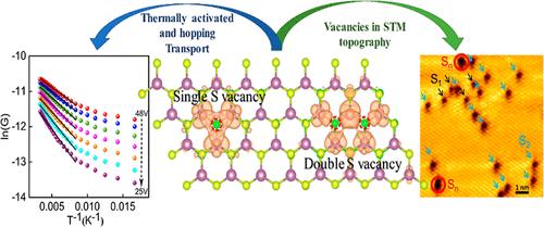
Defects in semiconductors play a crucial role in modifying their electronic structure and transport properties. In transition metal dichalcogenides, atomic chalcogen vacancies are a primary source of intrinsic defects. While the impact of these vacancies on electrical transport has been widely studied, their exact role remains not fully understood. In this work, we correlate optical spectroscopy, low-temperature electrical transport measurements, scanning tunneling microscopy (STM), and first-principles density functional theory (DFT) calculations to explore the effect of chalcogen vacancies in MoS2 monolayers grown by chemical vapor deposition. We specifically highlight the role of disulfur vacancies in modulating electrical properties, showing that these defects increase the density of shallow donor states near the conduction band, which facilitates electron hopping conduction, as evidenced by low-temperature transport and STM measurements. These findings are further supported by DFT calculations, which reveal that the electronic states associated with these defects are relatively delocalized, promoting hopping conduction and inducing n-type doping. This mechanism accounts for the observed high field-effect mobility (>100 cm2 V–1s–1) in the samples. These findings highlight the potential for defect engineering as a universal approach to customizing the properties of 2D materials for various applications.
揭示二硫化钼单层中缺陷与高迁移率之间的关系
半导体中的缺陷在改变其电子结构和输运性质方面起着至关重要的作用。在过渡金属二硫族化合物中,原子硫空位是固有缺陷的主要来源。虽然这些空位对电传输的影响已被广泛研究,但它们的确切作用仍未完全了解。在这项工作中,我们将光学光谱,低温电输运测量,扫描隧道显微镜(STM)和第一性原理密度泛函理论(DFT)计算相关联,以探索化学气相沉积生长的二硫化钼单层中硫空位的影响。我们特别强调了二硫空位在调制电学性质中的作用,表明这些缺陷增加了导带附近的浅层供体态的密度,这有利于电子跳跃传导,正如低温输运和STM测量所证明的那样。这些发现得到了DFT计算的进一步支持,表明与这些缺陷相关的电子态是相对离域的,促进了跳变传导并诱导了n型掺杂。这一机制解释了在样品中观察到的高场效应迁移率(>100 cm2 V-1s-1)。这些发现突出了缺陷工程作为一种通用方法的潜力,可以为各种应用定制2D材料的特性。
本文章由计算机程序翻译,如有差异,请以英文原文为准。
求助全文
约1分钟内获得全文
求助全文
来源期刊

ACS Applied Materials & Interfaces
工程技术-材料科学:综合
CiteScore
16.00
自引率
6.30%
发文量
4978
审稿时长
1.8 months
期刊介绍:
ACS Applied Materials & Interfaces is a leading interdisciplinary journal that brings together chemists, engineers, physicists, and biologists to explore the development and utilization of newly-discovered materials and interfacial processes for specific applications. Our journal has experienced remarkable growth since its establishment in 2009, both in terms of the number of articles published and the impact of the research showcased. We are proud to foster a truly global community, with the majority of published articles originating from outside the United States, reflecting the rapid growth of applied research worldwide.
 求助内容:
求助内容: 应助结果提醒方式:


