Sinan Bugu*, Sheshank Biradar, Alan Blake, CheeWee Liu, Maksym Myronov, Ray Duffy, Giorgos Fagas and Nikolay Petkov*,
{"title":"High-Fidelity TiN Processing Modes for Multigate Ge-Based Quantum Devices","authors":"Sinan Bugu*, Sheshank Biradar, Alan Blake, CheeWee Liu, Maksym Myronov, Ray Duffy, Giorgos Fagas and Nikolay Petkov*, ","doi":"10.1021/acsaelm.4c0149910.1021/acsaelm.4c01499","DOIUrl":null,"url":null,"abstract":"<p >Charge or spin-qubits can be realized by using gate-defined quantum dots (QDs) in semiconductors in a similar fashion to the processes used in CMOS for conventional field-effect transistors or more recent fin FET technology. However, to realize a larger number of gate-defined qubits, multiples of gates with ultimately high resolution and fidelity are required. Electron beam lithography (EBL) offers flexible and tunable patterning of gate-defined spin-qubit devices for studying important quantum phenomena. While such devices are commonly realized by a positive resist process using metal lift-off, there are several clear limitations related to the resolution and the fidelity of patterning. Herein, we report a systematic study of an alternative TiN multigate definition approach based on the highest resolution hydrogen silsesquioxane (HSQ) EBL resist and all associated processing modes. The TiN gate arrays formed show excellent fidelity, dimensions down to 15 nm, various densities, and complexities. The processing modes developed were used to demonstrate applicability of this approach to forming multigate architectures for two types of spin-qubit devices prototypic to (i) NW/fin-type FETs and (ii) planar quantum well-type devices, both utilizing epi-grown Ge device layers on Si, where GeSn or Ge is the host material for the QDs.</p>","PeriodicalId":3,"journal":{"name":"ACS Applied Electronic Materials","volume":"7 2","pages":"652–659 652–659"},"PeriodicalIF":4.7000,"publicationDate":"2025-01-10","publicationTypes":"Journal Article","fieldsOfStudy":null,"isOpenAccess":false,"openAccessPdf":"","citationCount":"0","resultStr":null,"platform":"Semanticscholar","paperid":null,"PeriodicalName":"ACS Applied Electronic Materials","FirstCategoryId":"88","ListUrlMain":"https://pubs.acs.org/doi/10.1021/acsaelm.4c01499","RegionNum":3,"RegionCategory":"材料科学","ArticlePicture":[],"TitleCN":null,"AbstractTextCN":null,"PMCID":null,"EPubDate":"","PubModel":"","JCR":"Q1","JCRName":"ENGINEERING, ELECTRICAL & ELECTRONIC","Score":null,"Total":0}
引用次数: 0
Abstract
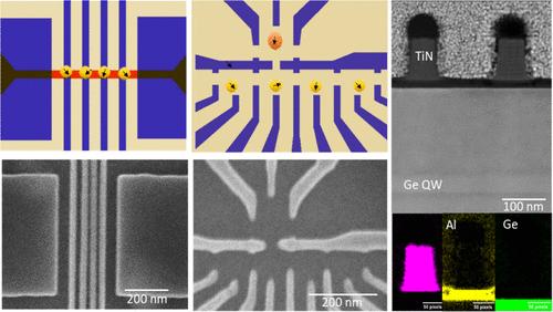
Charge or spin-qubits can be realized by using gate-defined quantum dots (QDs) in semiconductors in a similar fashion to the processes used in CMOS for conventional field-effect transistors or more recent fin FET technology. However, to realize a larger number of gate-defined qubits, multiples of gates with ultimately high resolution and fidelity are required. Electron beam lithography (EBL) offers flexible and tunable patterning of gate-defined spin-qubit devices for studying important quantum phenomena. While such devices are commonly realized by a positive resist process using metal lift-off, there are several clear limitations related to the resolution and the fidelity of patterning. Herein, we report a systematic study of an alternative TiN multigate definition approach based on the highest resolution hydrogen silsesquioxane (HSQ) EBL resist and all associated processing modes. The TiN gate arrays formed show excellent fidelity, dimensions down to 15 nm, various densities, and complexities. The processing modes developed were used to demonstrate applicability of this approach to forming multigate architectures for two types of spin-qubit devices prototypic to (i) NW/fin-type FETs and (ii) planar quantum well-type devices, both utilizing epi-grown Ge device layers on Si, where GeSn or Ge is the host material for the QDs.
期刊介绍:
ACS Applied Electronic Materials is an interdisciplinary journal publishing original research covering all aspects of electronic materials. The journal is devoted to reports of new and original experimental and theoretical research of an applied nature that integrate knowledge in the areas of materials science, engineering, optics, physics, and chemistry into important applications of electronic materials. Sample research topics that span the journal's scope are inorganic, organic, ionic and polymeric materials with properties that include conducting, semiconducting, superconducting, insulating, dielectric, magnetic, optoelectronic, piezoelectric, ferroelectric and thermoelectric.
Indexed/Abstracted:
Web of Science SCIE
Scopus
CAS
INSPEC
Portico

 求助内容:
求助内容: 应助结果提醒方式:


